光學實驗室
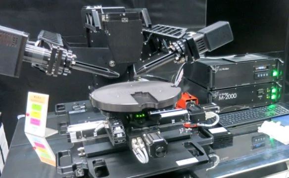
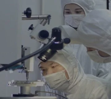
ASE Optical Laboratory provides wafer-level (WL) optical test solution and optical thin-film characterization & simulation.
Driven by emerging Telecom/Datacom demands and applications for high-performance computing (HPC) and artificial intelligence (AI), silicon photonics (SiPh) is a promising technology that provides greater bandwidth, low latency transmission over longer distance, low power consumption and high-level package integration. In order to meet future SiPh demands and applications, ASE developed comprehensive optical testing capabilities to support SiPh products development.
Wafer Level Optical Test
Capability
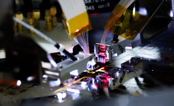
- Optical and electrical testing capabilities (Optical to Optical (O/O), Optical to Electrical(O/E)) for 200/300mm photonics wafers.
- Optical insertion loss (IL)/polarization dependent loss (PDL) spectrum sweep. Photodetector (PD) responsivity measurement*.
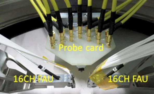
- Grating coupler test for various incident angles (eg. 8/10/12 deg.) with Single Mode Fiber (SMF) or multi-channel Fiber Array Unit (FAU) as optical probe.
- C-, L-, or O-band tunable laser (1240~1380nm/1490~1640nm) equipped with polarization synthesizer and multi-channel optical power meter.
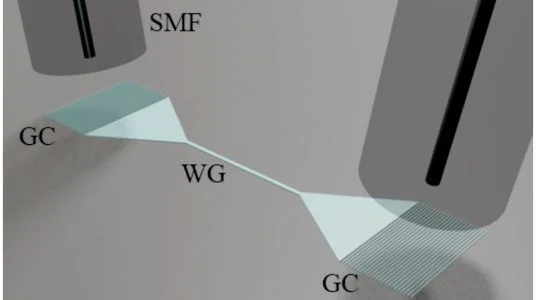
O/O testing with SMF
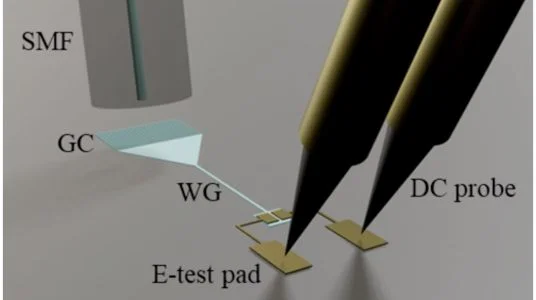
O/E testing with SMF and DC probe
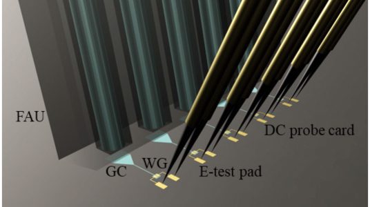
O/E testing with FAU and DC probe cards
Optical thin-film Characterization, Modeling and Simulation
Capability
- Transmittance/reflectivity
- Wavelength spectrum
- Dimension measurement
- Optical structure optimization
