
部落格
2.5D vs Fan-out Chip on Substrate
賴威宏
The demand for high bandwidth and high-performance applications such as networking, AI computing and GPU IC chips are driving innovative developments in advanced IC packaging. Heterogeneous integration enables the integration of multiple chips using fine line/space interconnect packaging technology.
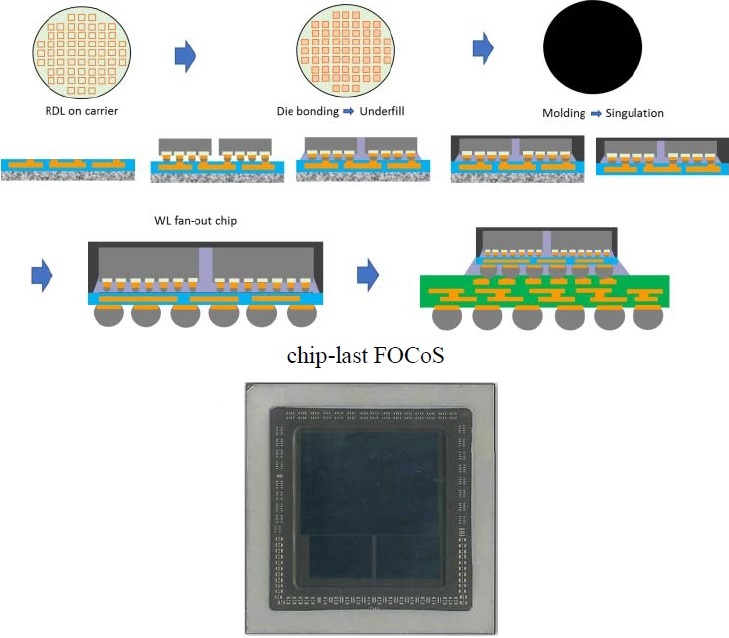
Heterogeneous integration packaging solutions offered in the market today include, through silicon via (TSV) interposer technology: 2.5D IC packaging and re-distribution layer (RDL) fan-out process better known as fan-out chip on substrate package (FOCoS).
FOCoS fabrication methods include chip first and chip last processes. We have utilized FEA simulations to examine the warpage, ELK layer crack risk, interconnection/RDL trace broken risk, and board level solder joint reliability of three package types: 2.5D IC, chip-first FOCoS and chip-last FOCoS. The validity of the simulation model is confirmed by comparing the numerical results for the warpage and thermal mechanical deformation of chip-last FOCoS with the experimental observations by advanced Metrology Analyzer (aMA) system. Further CFD simulations are then performed to investigate the heat dissipation performance of the three package types.
We have investigated the warpage and in-plane thermal deformation of packages at various environment temperatures. Three-dimensional numerical models have been developed to compare the mechanical and thermal performance. The warpage and inplane thermal deformation of the FEM model has been validated with the measurement result. Having validated the FEM model, this study applied the FEA investigations to package types’ comparison and examine the influence of the chip-last FOCoS wafer level underfill material properties on the D2D area interconnection copper trace reliability.
The results from the numerical simulation are as follows:
- The warpage of the two FOCoS package types are lower than 2.5D IC due to smaller CTE mismatch between combo die and stack-up substrate. Besides, the chip-last FOCoS has the lowest warpage quantity with the contribution of wafer level underfill.
- The ELK stresses of FOCoS for both chip-first and chip-last are lower than 2.5D package, because RDL/PI layers are the effective buffering to reduce ELK layer stress.
- The solder ball with maximum CSED occurs on the outermost solder joint located on the package edge of the solder joint top side, i.e. substrate side, surface. All these three packages have insignificant difference on CSED. It means that the board level TCT performance is similar because the equivalent CTE of all the package types are similar.
- The interconnection copper trace stress of 2.5D package has lower stress than others due to smaller localized CTE mismatch to reduce copper trace stress.
- The wafer level underfill type D with higher Tg and lower CTE has lowest stress, which could enhance copper trace reliability performance.
- 2.5D IC, chip-first FOCoS and chip-last FOCoS have similar thermal performance and all of them are good enough for high power applications.
More information can be found in the ECTC article entitled “A comparative study of 2.5D and fan-out chip on substrate: Chip first and chip last“.