
3D 系統級封裝
Driven by internet-of-things (IoT), edge computing, wearable and next generation wireless connectivity applications, more and more electronic components are assembled in a single unit to provide multiple functions associated with a system or sub-system. Initially, double side molding (DSM) technology is utilized to address the needs by assembling several die not only on one side of a substrate but on two sides (top and bottom) of the substrate. To further shrink package size and allow more function integration, ASE developed 3D System-in-Packages providing three or four-side assembly structure.
What is 3D System in Package (3D SiP)?
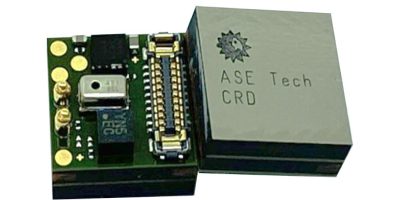
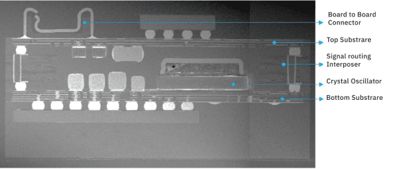
3D SiP is a very high-density assembly structure which provides three or four side assembly on top and bottom substrates interconnected by signal routing interposers there between to increase packaging density. Active component (fcCSP, WLCSP, silicon die, MEMS or etc..) and passive component (not only resistor, capacitor, inductor, but also X’tal* or oscillator) can be mounted on both sides of top and bottom substrates. It’s a highly integrated solution for small form factor and product modulation. Compared with double side SiP, 3D SiP can reduce more than 13% area, but only increase less than 10% thickness.

Assembly Process of 3D SiP
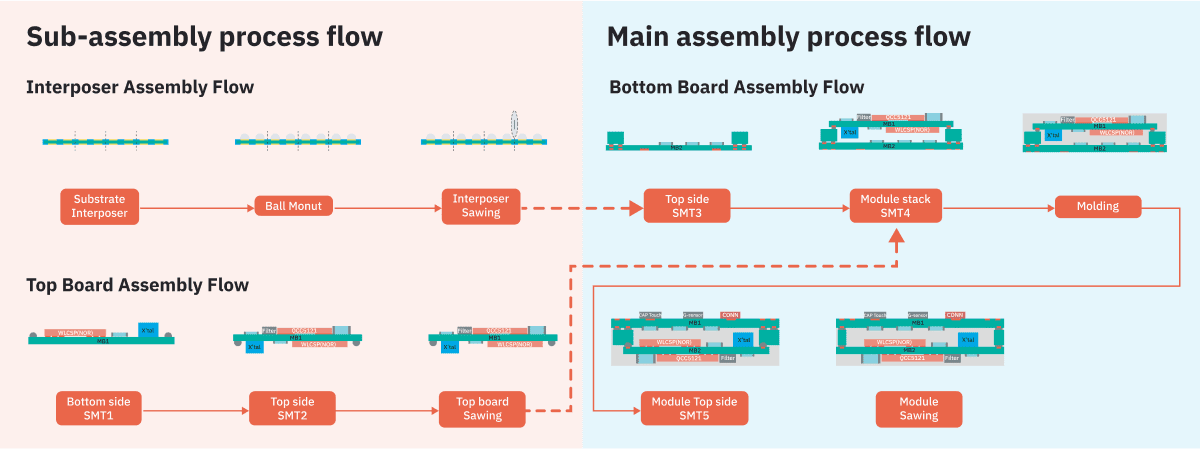
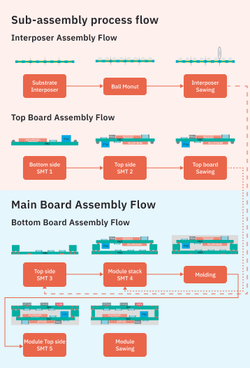
The 3D SiP assembly process can be simply divided into three phases: Interposer assembly, Top board assembly and Bottom board (Module) assembly. 3D SiP assembly methods include SMT, molding, sawing, and shielding process as illustrated below:
Key Advantages of Applying 3D SiP
- Smaller form factor
- Allow highly integrated electronic functionalities
- Better electrical performance

3D SiP Applications
3D SiP is ideal for 6*6mm² to 30*30mm² package size that are designed for wearable (watch, earphone), wireless charger, RF FEM, and Sensor system. The most advantages of 3D SiP are miniaturization and more function integration, therefore, 3D SiP is a good package platform to consolidate heterogeneous chips for performing multiple functions in a relatively smaller form factor.