天線封裝
Antenna in Package (AiP) or antenna on Package (AoP) has emerged as the mainstream antenna packaging technology for various millimeter-wave (mmWave) applications. ASE develops and offers cutting-edge AiP solutions through our leadership in SiP technology. We provide a complete suite of AiP manufacturing capabilities from system design, software development, module testing to electro-thermal simulation that enable our customers to develop smaller, higher performance, lower power consumption and more cost-effective mmWave products.
Introduction
Developments in 5G is advancing rapidly, and this 5th generation mobile network will transform the way we interact with our world by bringing a higher level of user experience over existing wireless technologies in terms of latency, reliability, efficiency, user and system capacity.
Today, each mobile device contains numerous communication modules that exchange wireless data with the external environment. In most 4G devices as well as sub-6GHz applications, antennas are manufactured in discrete form, e.g., as a printed shape on the PCB or as an individual component to be assembled near the RF front-end chip (transceiver) with an associated matching circuit. Thanks to significantly smaller antennas at mmWave frequencies, the antenna in the mmWave band can be directly integrated in the package. The industry is already developing new IC packages for 5G mmWave by combining the transceiver and the antenna in the same package to position the transceiver closer to the antenna to boost the signal.
What is Antenna in Package (AiP)?
AiP technology is an antenna packaging solution that implements an antenna or antennas in an IC package that can carry a bare RF chip (transceiver). The AiP can be further integrated with front-end components (e.g., power amplifiers (PA) or low-noise amplifiers (LNA), switches, filters and even power management integrated circuit (PMIC) to form an antenna module using System-in-Package (SiP) technologies. The SiP process applies double-side molding, selective molding, passive component integration, and various electromagnetic interference (EMI) shielding techniques.
A typical FCBGA AiP includes a RF chip (transceiver) attached to a package substrate with solder balls for connection to a main PCB. An array of antennas sits atop the upper portion of the package substrate, allowing wireless communication and detection. Flip-chip techniques are utilized to connect the RF chip to the substrate, thereby mitigating the interconnect loss.
Advantages of AiP
Compared with placing the antenna as a separate component on the system PCB, the key benefits of integrating an RF chip (transceiver) and the antenna into one package include:
Shorter interconnection between the antenna and the RF chip
- Improved signal integrity with reduced signal attenuation
- Addressing the range and propagation challenges that occur at higher frequencies
Reduced design difficulty at the system level*
- Greater design flexibility in product development
- Faster time to market
Small form factor
- Viable for 5G or IoT applications that require smaller package footprints
ASE mmWave AiP Offerings
ASE offers a variety of AiP solutions that leverage upon established Heterogeneous Integration (HI) capabilities to support the design of the next generation mmWave products. Each package solution aims to address design constraints such as electrical performance, thermo-mechanical reliability, compactness, manufacturability and cost.

Flip Chip Ball Grid Array (FCBGA) based AiP
FCBGA-based AiP includes an RF chip mounted on the bottom of a ball grid array (BGA) substrate and an antenna array formed on top of the substrate. We have designed a mmWave 28-GHz AiP using a FCBGA structure with 2x2 stacked patch antenna array formed on on a low-loss multilayer organic substrate*.
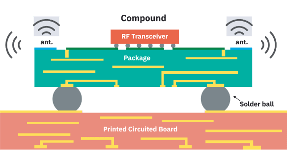
AiP Modules
In an AiP module designed for smartphones, the RF chip is mounted on top of a multi-layers (typically > 12 layers) antenna board with an antenna array formed on the bottom side thereof. It is designed to include a connector that simultaneously carries multiple high-frequency signals to the phone’s main board via a flexible printed circuit board.

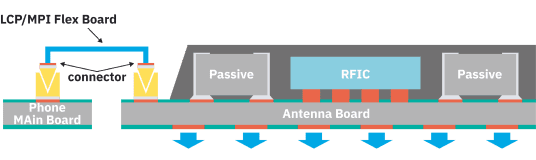
Hybrid-substrate based AiP
This packaging architecture is characterized by mounting the RF chip on top of a Hybrid-substrate including a typical BT substrate and an antenna flexible printed circuit (FPC). The antenna FPC is built from low dielectric constant (Dk)/dissipation factor (Df) materials that enable the lowest possible signal loss for high-frequency applications.
AiP Applications
As the antenna size can be small enough to fit into a small package, AiP technology is widely adopted in high-frequency applications such as 60-GHz radios and gesture radars, 77-GHz automotive radars, 94-GHz phased arrays, 122-GHz imaging sensors, 300-GHz wireless links as well as 5G mobile networks operating at mmWave frequencies (e.g., 28, 39, 60, 77 and beyond 90 GHz).
Precise AiP Measurement System
5G is poised to dominate the wireless world, but over-the-air (OTA) testing of 5G beamforming antennas, test validation of the antenna array integrated in 5G mmWave, and other antenna testing issues remain a challenge.
ASE, in collaboration with Keysight Technologies, has developed a leading-edge AiP measurement system which offers best-in-class measurement integrity and high repeatability that enable customers to transform advanced designs into competitive products. The AiP measurement system is designed to test various parameters in an AiP with precise accuracy and provides our customers an edge over the competition to deliver their products to market fast.
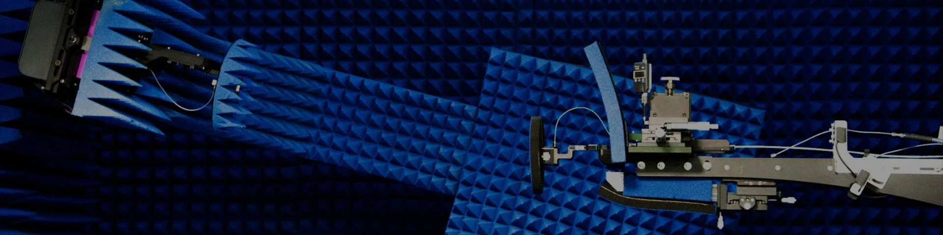
mmWave Antenna Measurement Chamber
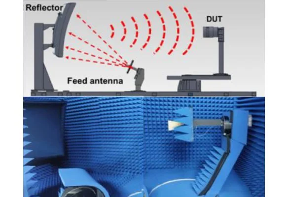
CATR – Compact Antenna Test Range
CATR – Compact Antenna Test Range
ASE mmWave Measurement Capability
S-Parameter Measurement
- PNA: 10MHz-67GHzn
- VDI Extension Module : 67GHz-115GHz
- Broadband frequency extender: 10MHz-110GHz
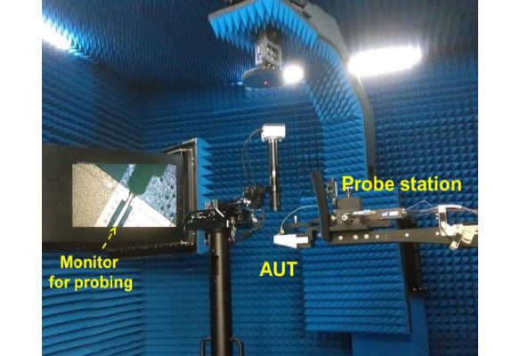
Probe-station
- 8” wafer level double-side measurement
- Panel level double-side measurement (600mmx600mm)