
扇出型系統級封裝
Furnishing every year’s new generation mobile with higher performance and smaller form factor, system in package (SiP) has become a certain path for innovation and an unstoppable trend for decade. Multi-functional active chips and related passive components are pre-assembled into a system or sub-system through heterogeneous integration design on laminated substrate. By the time when SiP was introduced to the mobile devices, new challenges emerged. Cost-effective integrated substrate became essential to achieve the sweat spot of consumer application. Small form factor is another key feature additional to the previous needs. As the existing technology has almost approached its limits, innovation is needed on the corresponding package of SiP for now and the future. Fan-Out re-distribution layers (RDL) can be an advanced substrate to break through the constraint so that RDL platform will be the core technology to evolve SiP to Fan-Out SiP.
Features of Fan-Out System in Package (Fan-Out SiP)
Several core technology building blocks including chip-last RDL manufacturing, carrier system, wafer level assembly and shielding sputtering enables Fan-Out SiP as illustrated in following figure. First, Fan-Out RDL provides fine line design capability which is better than mainstream substrates to enhance the function matching in SiP. Second, carrier system makes thin wafer handling possible. In addition, wafer level assembly delivers High-Speed (> 60 k units per hour) SMT service and Molded Underfill (MUF) technique for advanced encapsulation. Finally, shielding sputtering provides an option to apply on specific RF applications. In brief, ASE offers customers a complete toolbox to serve Fan-Out SiP packaging.
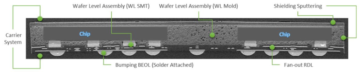
Cross-section of Fan-Out SiP and Technology Building Blocks

Benefits of Fan-Out SiP
- Flexible RDL Design to Tune System Performance (Compared to Wire Bonding)
- Finer RDL Line Width and Space for Higher Performance Control (Achieve about 5X Enhancement)
- Substrate Layer Reduction (about 3 Layers Cutdown)
- Cost-effective Process by Wafer Level Platform and High-Speed SMT Capability (Compatible with Bumping Process)
- Wider Radio frequency (RF) Application Based on Optional Shielding Technology (Five Side Sputtering)

Fan-Out SiP Applications
The available market approach scope can be categorized into: smartphones, tablets, RF infrastructures, edge computing, and internet-of-things (IOT) as shown in following figure. Higher frequency applications, better performance and cost-effectiveness are driving the innovation and integration of packages. Fan-Out SiP provides a new platform to fulfill the demand from these markets to make the next generation products possible.