系統級封裝
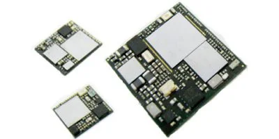
The drive towards semiconductor miniaturization and integration is rapidly unleashing the power and potential of System-in-Package (SiP), a package or module containing a functional electronic system or sub-system that is integrated and miniaturized through IC assembly technologies. ASE is the leader in System-in-Package (SiP) technologies from design to assembly and high-volume manufacturing while serving a broad spectrum of applications and markets. With attributes that deliver higher performance, cost-effectiveness, and shorter time to market, SiP technology is enabling functionality and creating opportunity across limitless electronics applications.
What is System-in-Package (SiP)?
ASE defines SiP as a package or module that contains a functional electronic system or subsystem that is integrated and miniaturized through IC assembly technologies. Rather than generic IC packaging technologies, development of SiP requires heterogeneous integration of single or multiple chips (such as a specialized processor, DRAM, flash memory), surface mount device (SMD) resistor/capacitor/inductor, filters, connectors, MEMS device, sensors, other active/passive components and pre-assembled package or subsystem.
Enabling Technologies
ASE’s SiP solutions leverage upon established IC assembly capabilities including copper wiring, flip chip packaging, wafer level packaging, fan-out wafer level packaging, 2.5D/3D IC and embedded chip packaging to address ongoing trends in mobile, IoT (Internet of Things), high-performance computing, automotive, and artificial intelligence.
Shielding
- Conformal Shielding
- Compartment Shielding
- Selective Shielding
- Magnetic shielding
Interconnection
- Cap Wire Bond
- Wire Bond
- Flip Chip
Die / Package Stacking
- 2.5D
- Die Thinning/Stacking
- Package on Package
- Package in Package
Antenna

Double Side Molding
- Double Side Molding
- Selective Molding
- Flexible Encapsulation
- Molded Underfill
- Irregular Packaging
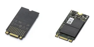
Wafer Level Package
Board Assembly
- High Density SMT
- ACF Bonding
- Wire Bond on Flex
- Laser Welding
- Flex Bending
Shielding
- Conformal Shielding
- Compartment Shielding
- Selective Shielding
- Magnetic shielding
Antenna

Double Side Molding
- Double Side Molding
- Selective Molding
- Flexible Encapsulation
- Molded Underfill
- Irregular Packaging
Board Assembly
- High Density SMT
- ACF Bonding
- Wire Bond on Flex
- Laser Welding
- Flex Bending
Interconnection
- Cap Wire Bond
- Wire Bond
- Flip Chip
Die / Package Stacking
- 2.5D
- Die Thinning/Stacking
- Package on Package
- Package in Package

Wafer Level Package
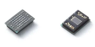
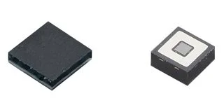
Conformal Shielding
ASE had introduced a novel conformal shielding technology (CFS) for electromagnetic interference (EMI) prevention, against external interference, keep chip normal working. For thinner, smaller and lighter product, PVD CFS technology was designed to substitute for metal can/lid. The technology was widely applied in wireless communication, ex: RF, Bluetooth, WiFi, etc.
Applications
- Phone/Tablet
- Wearable Device
- Glasses
- Camera
- Car System
Features
CPS technology was prevented package to package and outer signal interference. Developed advanced PVD process replaced metal can/lid to reach product miniaturization, area reduction 17% and thickness reduction 7%.
Capabilities
ASE developed PVD CFS technology was reached over 99.9% (SE value > 30dB) EMI impact in 0.5 to 6GHz frequency when metal layer thickness over 3um.
Compartment Shielding
ASE had introduced a new, EMI compartment shielding (CPS) structure which was constructed from laser trench and conductive paste. The technology is designed to provide better shielding performance in more compact structure. The distinctive characteristics of CPS technology (Laser trench/Conductive paste filling) are flexible and customized design for high-integration module. This offers customers much more aggressive layout design, and also high-level EMI shielding performance for sensitive components/chipset. In addition, CPS technology enables the smaller form factor of modules which is needs of wearable device, mobile device, and IoT application.
Applications
- Phone/Tablet
- Wearable Device
- Glasses
- Camera
- Car System
Features
- Higher EMI shielding performance
- Highly flexible and customized shielding pattern design
- Thinner, compact shielding barrier (~150um)
- Mold base compartment shielding solution
Capabilities
Structure:
- Trench opening width (top/bottom): 400um/80um
- Shielding performance (S.E.): 45~50dB (1GHz – 6GHz)
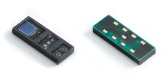
Antenna on Package
Antenna on Package (AoP) is a new approach to minimize the antenna size at the package level, which not only can provide the smallest antenna, but also a highly integrated RF SiP module to reduce the difficulty at the system level.
Applications
AoP technology allows much more applications in mobile device and wireless communication, such as 2.4GHz BLE in BT4.2 and future BT5.0, WiHD in IEEE 802.15.3c, WiGig in IEEE 802.11ad. In addition, AoP technology enables the advanced 3D patterning on package that addresses the need in the challenging 77GHz for car radar and 94GHz for imaging.
- Phone/Tablet
- Wearable Device
- Glasses
- Camera
- Car System
Features
AoP technology is designed to provide a good radiation performance with the low insertion loss and good impedance matching between the RF SiP and the antenna. Base on a completed material and process database system in ASE, the electromagnetic simulation can be performed for different customer requested conditions. The key to realize the optimum design into a successful AoP product is through the powerful 3D patterning ability on a conformal and good quality metal film.
Capabilities
ASE concentrates on advanced 3D patterning developing with high accuracy control and high automation throughput and these unique capabilities include:
- Min. package size: 4.9mm x 3.3mm (achieved at 2.4GHz)
- Film step coverage: >30%
- Min. line/space on top: 250μm
- Dimension tolerance on side wall: within +/-35um
High Density SMT
The ways to reduce form factor of SiP in X/Y size are utilization of tiny passive components and shrinking distance between components to component. ASE HD-SMT technology by using tiny 01005 SMD and 3 mils component to component distance is ready and in mass production.
To expand more functions in restricted body size of a SiP/module, dual side SMT as well as double sides molding technology is adopted.
Applications
- Phone/Tablet
- Wearable Device
- DGlasses, Camera
- DIoT/Smart Home Electronics
- DCar System
Features
- One side or dual side SMT
- Ultra-high accuracy pick & place
- Ultra-high SPI & AOI for yield insurances
Capabilities
- 01005 component MP, 008004 ready
- 6-layer 0.185mm substrate in mass production
- Minimum 3 mils component to component distance
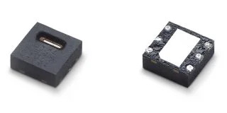
Selective Molding
ASE provides an advanced module encapsulation technology, called the selective molded module technology. It can solve the sensitivity components cannot put in over molded issue, but also allows the end product space design has greater flexibility.
Applications
Miniaturization module especially in WiFi and RF.
Features
On the same side of the substrate, there are both an mold area and a open area.
Capabilities
- Clearance of open area: > 0.3mm
- Clamp width between mold area and open area: > 0.6mm
- Clamp width between open area and package side line: > 0.6mm
Module Level
| Pre-con (L3) | TCT-1000 | HAST-264 | HTST-1000 |
| Passed | Passed | Passed | Passed |
Board Level
| Drop Test | Function |
| Passed | Passed |
Flexible Encapsulation
ASE provides an advanced encapsulation technology, called the flexible encapsulation technology. It enhances the wearable products in the waterproof function: products can still be bent after encapsulation.
Applications
Wearable electrical product including clothes, glasses, watches, bracelets, and rings.
Features
This technology uses a special flexible sealant material with a soft board (FPC) so that the module can be bending in the end product after module assembly.
Capabilities
| Test Item | Test Condition | Duration | Results |
|---|---|---|---|
| Pre-con (L3) | TCT-1000 | HAST-264 | HTST-1000 |
| TCT | -55°C~85°C | 100 cycles | Passed |
| Bending | 30°C | 100 cycles | Passed |
| Twist | twist span 45mm, angle 5~30 degrees | 100 cycles | Passed |
Turnkey Solution
ASE offers customers complete SiP manufacturing capability including system design, software development, module testing and electrical heat transfer simulation technology to enable smaller, higher performance, lower power consumption and more cost-effective end products.
System Co-Design
- SiP Electronic Design Automation (EDA) solution
- RF Circuit design
- Antenna Design
- Shielding Solution
- Substrate Layout design
Packaging Consultancy
- Package selection & configuration
- Design rule guideline
- Process capability
- Reliability verification
System Test Consultancy
- RF Wafer probing
- RF ATE Platform
- EVB design & fabrication
- Testing tooling design
- Final test solution development
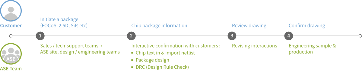
System-in-Package Intelligent Design (SiP-id)
SiP-id stands for System-in-Package – Intelligent Design. The solution consists of an enhanced reference flow that includes IC packaging and verification tools from Cadence, and a new methodology that aggregates the requirements of wafer-, package- and system-level design into a unified and automated flow. By deploying the SiP-id methodology, chip designers can reduce design iterations and greatly improve throughput as compared to existing advanced packaging EDA tools. The end result is a vast reduction in the time needed to design and verify ultra-complex SiP packages.
It is our intention to offer all ASE customers a set of efficient tools where designers can freely experiment with designs which can go beyond the current packaging limits. This set of design tools are available to eligible customers immediately. However, some of the proprietary libraries and design rules will be subject to an agreement with ASE. It is our belief that IoT, AI, VR, AR, EV and all future applications will demand more SiPs and modules. This is an ongoing effort by ASE, not only to develop fanout (such as Fan-Out Chip on Substrate, FOCoS), panel fanout, embedded substrates, 2.5D, but also to making design tools more user-friendly, up-to-date and efficient.
What is required to start a package design with SiP-id, DRC deck is required for fan-out design and 3D DRC deck, for SiP design. The customer can engage our in-house engineering to begin the process.
SiP Applications
SiP solutions are highly adopted by end customers for applications including wireless communication, computer storage, power and sensor. In addition, ASE SiP solutions enable a wide range of smart applications including smart living, smart bike, smart city, smart automotive and smart hearables. Advanced SMT, encapsulation, shielding as well as interconnection assembly technologies are developed to meet future requirements arising from 5G communication, AR/VR sensing, and health caring applications.
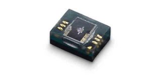
BT/BLE+MCU SiP Module
Applications
- Remote Control
- Health, Fitness and Medical Devices
- Home Automation, Energy
Features
- 2.4 GHz BLE transceiver
- ARM®sup> Cortex – M0 32 bit processor
- 256 kb embedded flash program memory
- 16 kb RAM
- Dimension: 6.5x6.5x1.2mm
- Package: AoP, LGA
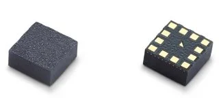
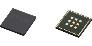
WLAN+MCU SiP Module
Applications
- IoT
- Smart Home
- Security
- Energy Harvesting
Features
- Dimension: LGA 11x11mm²
- Structure: FC+W/B
- WiFi 11b/g + 32bit MCU (50MHz)
- 128kb flash + 512kb EEPROM
- Dimension: 6.5x6.5x1.2mm
- Protection: molding, conformal shielding
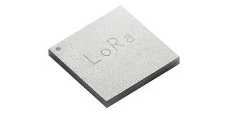
LoRa/SigFox/NB-IoT SiP Module
Applications
- Wireless Alarm and Security Systems
- Internet of Things (IoT)
- Smart City
Features
- SX1276 transceiver
- Intel 32MHz Quark MCU
- DSP for sensor subsystem
- Worldwide LoRa ISM band embedded
- 384 kb of on-die NVM+8 kb OTP on-die NVM
- 80kb of on-die SRAM
- Dimension: 12x12x1.3mm
- Package: Conformal shielding, WLCSP