扇出型封裝
Fan-Out packaging continues to gain prominence within the industry, based on significant technical advantages that have led to its broad commercialization. As we move further into the era of system-in-package (SIP) and heterogeneous integration, Fan-Out packaging will become increasingly significant. ASE is evolving this advanced packaging platform to meet application demands for smaller form factors and improved electrical and thermal performance.
What is Fan-Out Packaging?
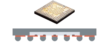
Literally speaking, “Fan-Out” packaging can be defined as any package with connections fanned-out of the chip surface, enabling more external I/Os. Conventional fan-out packages use an epoxy mold compound to fully embed the dies, rather than placing them upon a substrate or interposer. Fan-Out packaging typically involves dicing chips on a silicon wafer, and then very precisely positioning the known-good chips on a thin “reconstituted” or carrier wafer/panel, which is then molded and followed by a redistribution layer (RDL) atop the molded area (chip and fan-out area), and then forming solder balls on top.
A popular packaging technique now is to build packages with a standard Fan-Out type RDL, but with dies embedded in materials such as organic laminate or silicon wafer instead of the mold compound. Please refer to “Embedded die packaging” for more details.
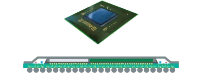
Fan-Out is a wafer-level packaging (WLP) technology. It is essentially a true chip-scale packaging (CSP) technology since the resulting package is roughly the same size as the die itself. When dealing with shrinking pitch design requirements, Fan-In WLP faces processing challenges as the area available for I/O layout is limited to the die surface. Fan-Out WLP, however, does not have this limitation as the technique allows for the redistribution of I/Os beyond the die surface and onto the over-mold which, in turn supports a thinner package.
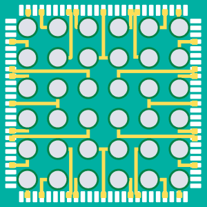
Fan-In WLP
All RDL traces are routed in towards the center of the die
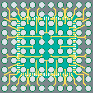
Fan-Out WLP
RDL traces are routed both inwards and outwards beyond the limits of the die
Features of Fan-Out Packaging
- Die Shrinkage: Fan-Out allows ball placement beyond the die area
- Heterogeneous & Homogeneous Integration: Excellent electrical connectivity
- System in Package (SiP): Ability to combine multiple dies and components such as MEMS, filters, crystals and passives in a relatively small size package
Comparative Advantages:
vs Flip-Chip Packaging
- Slightly smaller footprint
- Lower profile
- Better electrical performance
- Better thermal performance
- Substrate-less package
- SiP and 3D integration advantage
vs Fan-In WLCSP
- Higher board-level reliability
- Fan-out area to counter the pad limitation issue, adaptable to customer needs
- The use of known good die (KGD)
- Better thermal performance
- Built-in back-side protection
- No restriction in bump pitch
- SiP and 3D integration advantage
Fan-Out Structures/Processes
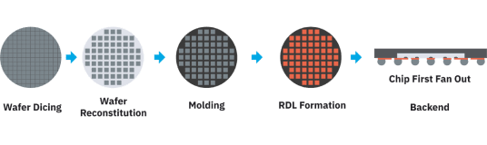
(I) Chip-First
The chips are first embedded in a temporary or permanent material structure, followed by the RDL (Redistribution Layer) forming processes. The Chip-First process provides a lower cost solution suitable for low I/O applications. However, the Chip-First process faces challenges of die shift, die protrusion, wafer warpage and RDL scaling, which limits its usage for complex multi-chip packaging and system-in-package (SiP) with passives integration.
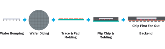
(II) Chip-Last
Also known as RDL first: the chips are not integrated into the packaging processes until the RDL on the carrier wafer are pre-formed. The Chip-Last process has less KGD (known good dice) yield concerns compared with the Chip-First process. Furthermore, in Chip-Last, molding is conducted after chips are secured on the RDL with flip chip bonds, thereby eliminating die shift, die protrusion and wafer warpage issues during the RDL fabrication, and allows the fabrication of fine pitch RDL on the carrier wafer. Chip-Last has better electrical performance and allows ultra-fine pitch scales e.g. 2um as well as small through-via capabilities.
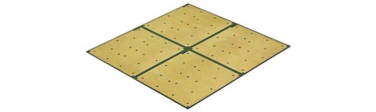
(III) Panel FO
Both of the previous mentioned processes utilize the round wafers as the reconstituted carrier for supporting the chips, the RDL and the molding process. By using a rectangular panel as the reconstituted carrier, panel level fan-out (Panel FO) offers the potential for lower production cost due to higher area utilization ratio of the carrier and better economical manufacturing, especially for large packages.
ASE Fan-Out Package Offerings
eWLB
BB, RF, Codec, Car Radar
- Pkg ~ 12x12
- RDL 12/12um
- 2L RDL
- Since 2009
eWLB (embedded wafer-level ball-grid array), also known as ASE aWLP: Chip-First, Face-Down, licensed from Infineon.
FOCoS
Networking, Server
- Pkg ~ 67x67
- RDL 2/2um
- 3L RDL
- Since 2016
FOCoS (Fan-Out Chip on Substrate): ASE In-house developed technology.

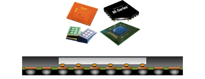
M-Series
RF, BB, PMIC, Codec
- Pkg ~ 12x12
- RDL 8/8um
- 2L RDL
- Since 2018
M-Series: Chip-First, Face-Up, licensed from Deca Technologies.
FOSiP
RF, FEM, Power, MCU
- Pkg ~ 15x15
- RDL 5/5um
- 5L RDL
- Since 2017
FOSiP (Fan-Out System in Package)

FOPoP
AP & Memory
- Pkg ~ 15x15
- RDL 5/5um
- 3L RDL
- Since 2016
FOPoP (Fan-Out Package on Package)
Panel FO
RF, FEM, Power, Server
- Pkg ~ 67x67
- RDL 2/2um
- 5L RDL
- Since 2019
Panel FO (Panel level Fan-Out): 300 x 300 mm panels for high-density solution (Chip-Last), 600 x 600 mm panels for low-density solution (Chip-First)
Fan-Out Packaging Applications
Fan-Out packaging is mainly driven by mobile applications, which require high-performance, energy-efficient thin- and small-form-factor packages. Today, fan-out is in high volume applications for a wide variety of products, including PMICs, RF packages, Baseband processors, and high-end networking systems.
New Fan-Out Opportunities for High Frequency:
Automotive Radar (76-81GHz)
5G Backhaul (>20GHz)
5G Fronthaul (>20GHz)
WiGig (60GHz)
Antenna in
Package (AiP)