2.5D and 3D IC Packaging
As 5G, AI, and high-performance computing continue to make inroads into our world, there’s escalating demand for semiconductor devices that deliver enhanced performance, lower latency, increased bandwidth and power efficiency. 2.5D & 3D technologies deliver that, and more. ASE continues to push boundaries by innovating the 2.5D & 3D technologies that are becoming more and more crucial within the industry. ASE has well-established itself as a leader in 2.5D technology, having successfully delivered pioneering 2.5D solutions that helped bring advanced ASIC and HBM products to the market place. To continue this technology innovation momentum, ASE is introducing high-density Fan Out technology for die stacking & multi-die solutions to achieve high bandwidth & high performance across the market landscape, addressing demand from high-density data centers to consumer & mobile space.
What is 2.5D & 3D IC Packaging?
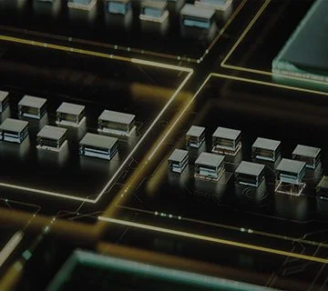
2.5D / 3D are packaging methodology for including multiple IC inside the same package. In 2.5D structure, two or more active semiconductor chips are placed side-by-side on a silicon interposer to achieve extremely high die-to-die interconnect density. In 3D structure, active chips are integrated by die stacking for shortest interconnect and smallest package footprint.
In recent years, 2.5D & 3D has gained momentum as an ideal chiplet integration* platform due to their merits on achieving extremely high packaging density and high energy efficiency.
ASE is one of the pioneers in 2.5D/3D packaging technology and has successfully launched world’s first mass production of 2.5D IC package equipped with High Bandwidth Memory (HBM).

Benefits of 2.5D & 3D IC Packaging
Our 2.5D/3D IC packaging solution provides the benefit of integrating GPU, CPU and memory along with decoupling capacitor. Si interposer with TSV (Through Silicon Via) can be used as a platform to bridge fine pitch capability gap between assembly substrate and integrated circuit board. It also helps to keep pad pitch scaling path without being limited by assembly substrate technology.
Key advantages of applying 2.5D & 3D IC Packaging:
- Ultra high routing density (L/S: 0.4/0.4µm)
- Ultra high I/O density (> 400 µbumps/mm²) & I/O pitch scalability
- Homogeneous / heterogeneous memory, power and/or optics integration
- Interposer capable of embedding decoupling capacitor or active devices feasible
- Excellent package reliability to meet automotive requirements

2.5D & 3D IC Applications
2.5D/3D IC packaging is mainly used to integrate HBMs of the following applications:
- High-end GPU
- High-end FPGA
- Network switch / router for data center & 5G infrastructure
- AI accelerator for AI training
In the era of chiplet, 2.5D & 3D IC packaging will play more and more significant roles in applications such as CPU, Mobile AP, Si photonics, display driver IC and lots more.