Flip Chip Packaging

Flip chip derived its name from the method of flipping over the chip to connect with the substrate or leadframe. Unlike conventional interconnection through wire bonding, flip chip uses solder or gold bumps. Therefore, the I/O pads can be distributed all over the surface of the chip and not only on the peripheral region. The chip size can be shrunk and the circuit path, optimized. Another advantage of flip chip is the absence of bonding wire reducing signal inductance.
An essential process for flip chip packaging is wafer bumping. Wafer bumping is an advanced packaging technique where ‘bumps’ or ‘balls’ made of solder are formed on the wafers before being diced into individual chips. ASE has invested significantly in the research and development as well as in equipment for wafer bumping. It has the capacity to bump 6-inch, 8-inch and 12-inch wafers.
Benefits of Flip Chip
-
Shorter assembly cycle timeAll the bonding for flip chip packages is completed in one process.
-
Higher signal density & smaller die sizeArea array pad layout increases I/O density. Also, based on the same number of I/Os, the size of the die can be significantly shrunk.
- Good electrical performanceShorter path between die and substrate improves the electrical performance.
-
Direct thermal dissipation pathExternal heat sink can be directly added to the chip to remove the heat.
-
Lower packaging profileAbsence of wire and molding allows flip chip packages to feature lower profiles.
Capabilities
ASE offers several BGA packages using flip chip technology. There are:
| I/O | Package Size(mm) | Substate | Ball Pitch(mm) | |
|---|---|---|---|---|
| CCSP | 16 ~ 200 | 4x4 ~ 14.0x22.0 | 2/4 Layer Laminate | 0.5 ~ 1.00 |
| Ceramic FCBGA/PGA | < 1556 | 27x27 ~ 49.5x49.5 | Ceramic | 0.8 ~ 1.27 |
| FCGBA | 100 ~ 1521 | 27x27 ~ 40.0x40.0 | 2/4 Laminate, 4-8 Layer Build-up |
1.0/1.27 |
| HFCGBA | 256 ~ 2401 | 12x12 ~ 52.5x52.5 | 4-8 Layer Build-up | 1.0/1.27 |
The thickness and the available ball count of flip chip packages are mostly customized. ASE provides several options for enhancing the performance of flip chip packages. They are:
Overall molding (for FCCSP)
The molding is used to protect the chip, substitute underfill for lower cost and improve the thermal performance and 2nd level reliability.
Heat spreader (for FCBGA)
The heat spreader provides direct heat conduction by adhering to the rear side of the silicon chip. This method provides 6~8W of thermal dissipation under natural convection.
ASE Flip Chip Packaging Offerings
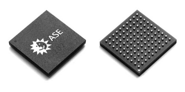
FCCSP (Flip Chip Chip Scale Package) offers chip scale capacity for I/Os around 200 or less. FCCSP provides better protection for chip and better solder joint reliability compared with direct chip attach (DCA) or chip on board (COB). FCCSP is more superior to known good die (KGD) in low-cost test and burn-in, and performs comparable electrical function with KGD. FCCSP features thin and small profile, and lightweight packages.
Applications
Consumer
- Camcorders
- Digital Camera
- DVD
Computer
- Voltage Regulators
- High-speed Memory
- Card
- PC Peripherals
Telecommunication
- Pagers
- Cellular Handsets
- GPS
Features
BGA is suitable for high power and high speed ICs requiring superb electrical and thermal enhancement.
- Thinner Profile: “Wafer Thinning” capability (down to 6~8 mils) to support packages thinner than 1.0 mm
- Substrate: 2-layer BT laminate substrate is used to reduce overall package cost
- Improved Performance: Thin core (100um) substrate & via-on-pad design can be adopted to achieve better electrical performance
- Robust Structure: Over molded process can enhance throughput, component and board level reliability
- NSMD with OSP C4 pad: Low cost solutions for electric interconnect between solder bump and substrate
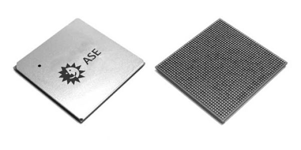
Flip Chip Organic BGA
Laminate or build-up organic substrate offers better electrical performance than wire-bond type BGA package especially in high frequency applications.
Flip Chip Ceramic BGA
Alumina ceramic substrate offers better moisture resistance, electrical insulating property and higher thermal conductivity than organic substrate. FCBGA is used primarily for high-reliability commercial applications (e.g. CPU).
Applications
Consumer
- Graphics/Chipsets for PC
- Server
- High-end Application
- Microprocessor for PC & Server
Telecommunication
- Network Products (LAN)
- Switching
- Transmission
- Cellular Base Stations
Features
HSBGA is suitable for high power and high speed ICs requiring superb electrical and thermal enhancement.
- Substrate: 4 layer laminate, 4~12 layer build-up, ceramic, and PTFE substrates are available
- Thermal Lids: Heat spreaders made of Cu with Ni plating, Aluminum, Ceramic, AlSiC
- Passive Component: Passive component attaching. It can be placed on the top or bottom side of the package
- Ceramic BGA: High Pb solder ball with eutectic solder paste improves board level reliability performance of ceramic packages

HFC BGA (High Performance FCBGA), a thermally enhanced FCBGA, is the composite package of FCBGA with heat spreader made of Cu, Al, or AlSiC. The heat spreader is used to extend the heat conduction area by connecting itself to the rear side of the silicon chip.
This method desensitizes the performance deviation out of the chip size, lowers the thermal resistance of junction-to-case (θjc) and enables the external heat sink or fan to work more effectively. HFCBGA can produce 6~8 watts of power dissipation under natural convection.
Applications
Consumer
- Graphics/Chipsets for PC
- Server
- High-end Application
- Microprocessor for PC & Server
Telecommunication
- Network Products (LAN)
- Switching
- Transmission
- Cellular Base Stations
Features
HSBGA is suitable for high power and high speed ICs requiring superb electrical and thermal enhancement.
- Substrate: 4 layer laminate, 4~12 layer build-up, ceramic, and PTFE substrates are available
- Thermal Lids: Heat spreaders made of Cu with Ni plating, Aluminum, Ceramic, AlSiC
- Passive Component: Passive component attaching. It can be placed on the top or bottom side of the package
- Ceramic BGA: High Pb solder ball with eutectic solder paste improves board level reliability performance of ceramic packages