FOCoS-Bridge
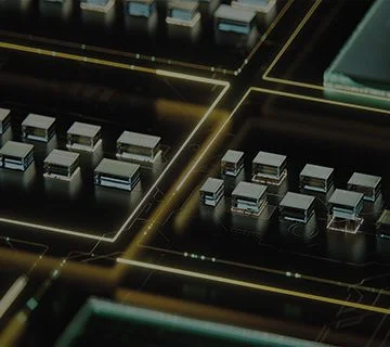
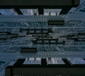
AI has penetrated nearly all industries and scientific disciplines, from autonomous vehicles to medical diagnostics. The convergence of AI and HPC is having a strong impact on the semiconductor industry, fueling demand for innovative packaging solutions. As AI and HPC applications continue to grow in sophistication, the demand for data transfer will continue to increase. FOCoS-Bridge technology is a promising semiconductor packaging solution that can help to meet the increasing demand for higher bandwidth and faster data transfer rates in AI and HPC applications. It leverages the advantages of highly integrated fan-out structures to overcome the limitations of traditional electrical interconnects, and enables high-speed, low-latency, and energy-efficient data communication between processors, accelerators, and memory modules.
What is FOCoS-Bridge?
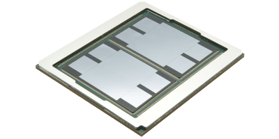
Positioned under the ASE VIPack™ platform, we offer a silicon bridge technology for implementing chiplet integration called Fan-Out-Chip-on-Substrate-Bridge (FOCoS-Bridge), which utilizes tiny silicon pieces with routing layers as in-package interconnect between chiplets, e.g, graphics computing chips (GPU) and high bandwidth memory (HBM). The silicon bridges are embedded in the fan-out RDL layer as detailed below.
FOCoS-Bridge is positioned as an alternative to 2.5D packages using silicon interposers. Like 2.5D, silicon bridges provide ultra-fine pitch interconnection in packages, which can address the memory bandwidth bottleneck challenges in systems. Compared with 2.5D, the advantages of FOCoS-Bridge is that we only use silicon pieces in the areas where we are trying to connect two chiplets together.
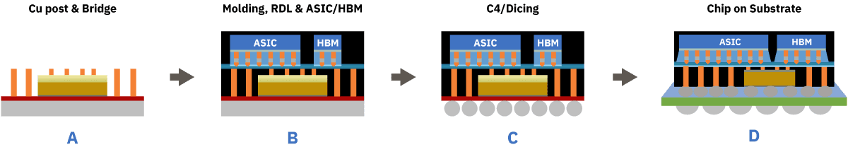
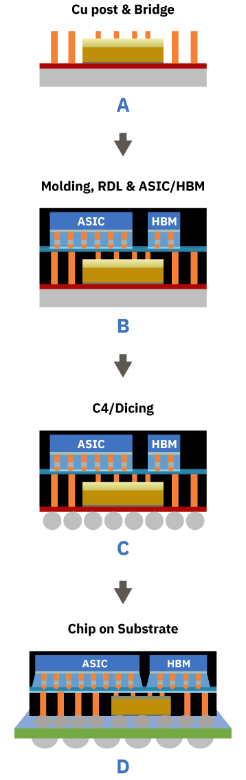
Fabrication Process of FOCoS-Bridge
As shown in Fig. A below, the to-be-embedded Si bridge die with micro-bumps thereon was attached to a wafer carrier, followed by Cu posts plating on the wafer carrier. Subsequently, a first molding process was conducted, the molded product is ground to expose the Cu posts and the micro-bumps, and then RDL layers were formed thereon. After that, ASIC and HBM dies were attached, followed by underfilling and second molding (see Fig. B). After the wafer carrier was removed and C4 bumps were formed, the molded wafer was sawn into individual fan-out packages (see Figure C). Finally, the fan-out package was attached to an organic substrate using conventional flip chip process (see Fig. D).
Benefits of FOCoS-Bridge
FOCoS-Bridge technology provide similar electrical, signal, and power integrity performance to silicon interposer solutions, but at a lower cost and without reticle size constraint. FOCoS-Bridge technology is designed to be highly scalable, enabling seamless integration into complex chip architectures while delivering high density die-to-die (D2D) interconnections with submicron L/S, high input/output (I/O) counts, and high-speed signal transmission for evolving Artificial Intelligence (AI) and High-Performance Compute (HPC) requirements. The use of a silicon bridge die enables a die edge linear density (wire/mm/layer) that is an order of magnitude higher than the traditional organic flip chip package. In addition, FOCoS-Bridge establishes the foundation for embedding passives and active chips in the fan-out package and provides options of decoupling capacitor integration for power delivery optimization and active dies for direct access to certain functions, such as memory, I/O, and more.
FOCoS-Bridge Applications
FOCoS-Bridge technology helps enable more efficient utilization of computing resources, accelerates data-intensive workloads, and contributes to the advancement of AI algorithms, deep learning, scientific simulations, and other computationally demanding tasks.
- Multi-die and HBM integration for AI, data center, server and networking applications
- Memory and passive integration for APU/CPU/GPUs and chiplets for applications across AI, data center, mobile, auto processors, communication infrastructure and networking

To download the FOCoS-Bridge Tech Brief, please complete the following form: