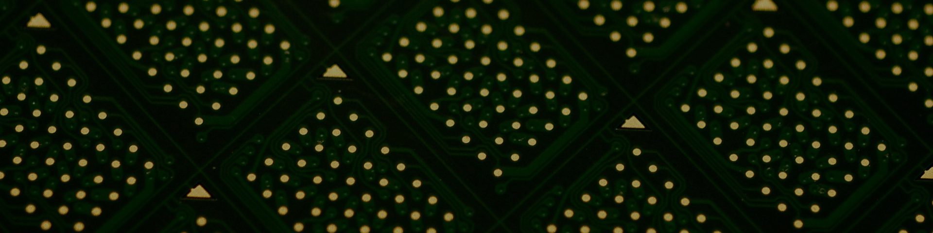
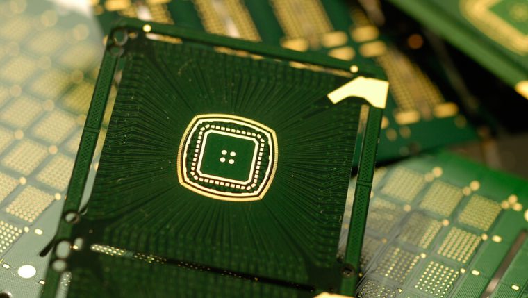
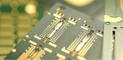
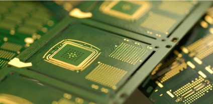
Substrate Design
As customers are demanding small, thin, and high performance for their electronic products, device makers are searching for high performance, high reliability, and low cost solutions. Substrate/lead frame has played a very important role in packaging industry, not only because it represents a great portion of the cost, but also because it has a great influence on package performance. How to design a high performance, low cost substrate/lead frame has become one of the major tasks in all packaging companies. In ASE, we have a group of experienced professional dedicate in substrate/lead frame design in order to provide turnkey solutions for our customers to fulfill high performance, cost saving and short time to market.
Function & Service
- Transmittance/reflectivity
- Color temperature (CCT)
- Illuminance (Lux)
- Optical structure optimization
- Light efficiency. View angle analysis
- Light Intensity & distribution
- Chromaticity coordinate (CIE)
- Color rendering index (CRI)
- Intensity & distribution analysis
- Module signal. Cross talk analysis
- Wavelength spectrum
- Luminous flux (lm)
- Dimension measurement
- Color analysis
Design Tool
The characteristics of packaging material are a major concern when determining how well the ICs will perform. ASE's Material Laboratory provides the characterization analysis of the following properties. The related instruments are listed next. Users can find more information from the Measurement Equipment section.Design information format
- GDS II
- Microsoft office format netlist
- Pad coordinator
- Ball out
Design tool
- Cadence
- Xynetix
Drawing offering
Layout Drawing:
- AutoCad R14
- 2000 Gerber RS 274X
- Acrobat pdf Format
Bonding Diagram:
- AutoCad R14, 2000
- Acrobat pdf Format