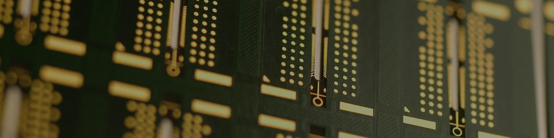
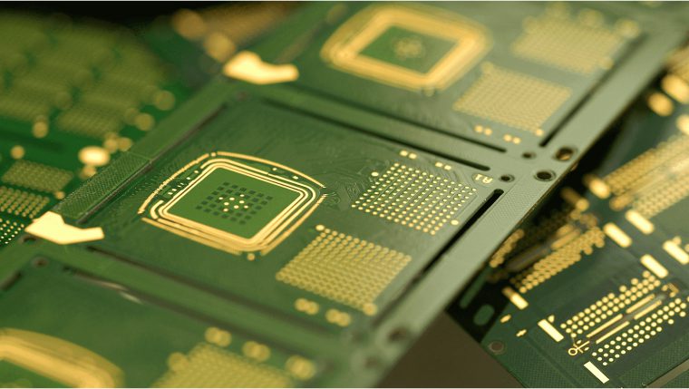
Packaging Substrate
Developments in the IC industry have triggered the rapid growth of the computing, communications and consumer electronics market in the last decade. Recently, the outsourcing trend has thrived in semiconductor backend services and the substrate business is a necessary complement to the assembly service of ICs. Continuing the momentum, ASE has focused on the research and development of substrate technology for low cost, high performance, thin, miniature, reliable and environmentally compatible next generation IC package solutions.
We expect substrates will become an increasingly important value-added component of the semiconductor packaging business. The demand for higher performance semiconductors in smaller packages will continue to spur the development of advanced substrates that can support the advancement in circuit design and fabrication. As a result, we believe that the market for substrates will grow and the cost of substrates as a percentage of the total packaging process is getting more significant, especially for advanced packages such as flip-chip BGA packages.
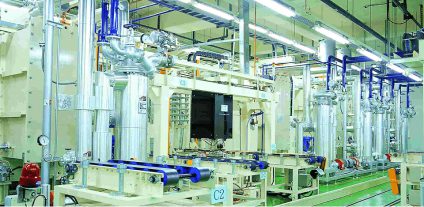
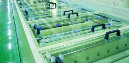
We leverage the expertise of ASE's capabilities to achieve integrated design by integrating the assembly technologies and substrate technologies as well as to provide our customers with reliable quality, cost effectiveness and fast cycle time. ASE well prepares in stable high volume manufacturing ability with consistently increasing capacity for customers' quick ramp up.
ASE's substrate design and manufacturing capability enables the interconnection materials of a wide range of wire-bond BGA and flip chip product applications. We also provide stub-less solutions * such as etching back、a-SG (advanced selected gold) and DPS (double pattern sputter) for high frequency and high performance package applications.
We believe that interconnect technology and materials have become an increasingly value-added element for the semiconductor packaging business. Consequently, ASE continues to focus on developing and enhancing the in-house capability and capacity of substrate design and manufacturing to benefit our customers with our fast cycle time, largest capacity, mature technology and competitive price.
ASE Packaging Substrate Offerings
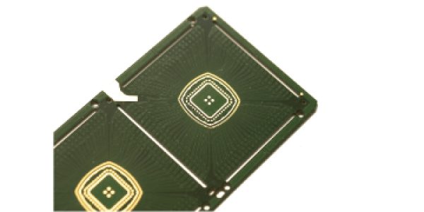
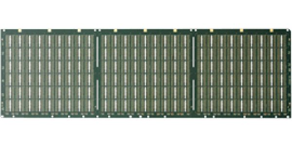
PBGA (Plastic Ball Grid Array) package consist of wire-bonded die on base substrate made up of glass fiber immersed resin copper clad laminate and encapsulate it by plastic (epoxy molding compound). ASE is capable of providing substrate suitable for high power and high speed package requiring enhanced thermal and electrical performance.
Applications
- Microprocessors/Controllers
- Gate Arrays
- Automotive applications
- ASIC
- PLDs, DSPs
- Digital TV
- Graphics and PC Chipsets
- Communications & Networking
- Medical
Features
- Low assembly cost
- Available in thinner substrate by using thin core
- High reliability and quality for Automotive
- High interconnect density
- Stub less solution (Etch back, a-SG, DPS process)
- Flexible sizes ranging from 15x15mm to 45x45mm
- Multi-layer options for signal, power and ground plane's electrical performance improvement
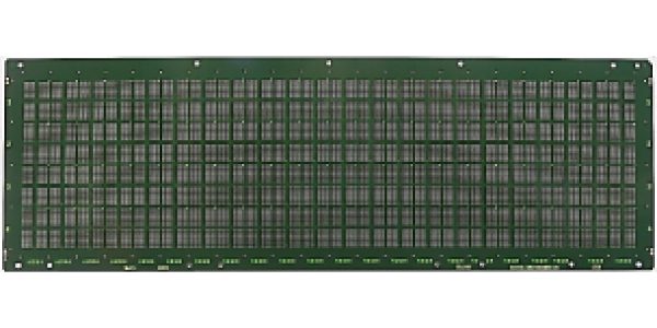
Semiconductor builds solder on bump side, and then mounts on Flip Chip substrate. Substrate is made by Chip side Embedded structure.
Applications
- Application Processor
- Bluetooth
- Networking
- Modem
- Connectivity
Features
- Thinner thickness structure (coreless)
- Cost effective solution
- Advance pattern design with fine line capability in the embedded layer
- Higher density of interconnects
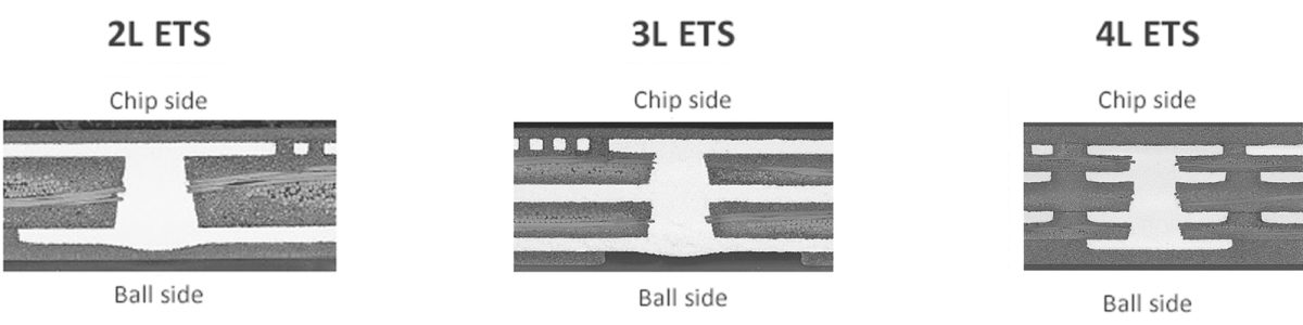
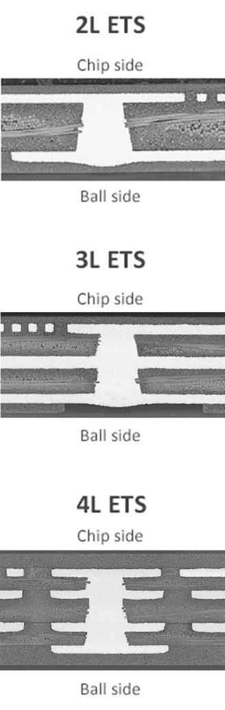
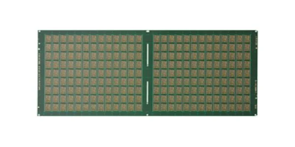
Embedded Trace Substrate (ETS)
The BOC package was designed as a cost effective CSP solution specifically for high-frequency memory devices. The structure provides the shortest wire length and outstanding electrical performance for the central – pad device layout through the use of low-cost wire bonding and BGA technologies.
Applications
The BOC package is an ideal IC package for devices such as SDRAM, SGRAM, DDR SDRAM, RAMBUS DRAM and next-generation.
Features
- Cost competitive for high performance DRAM
- Dielectric- Rigid 2 layer substrate
- JEDEC standard configuration – 60 balls
- Customer substrate design available
- Package dimension 1.2mm max thickness
ASE is committed in providing a reliable memory substrate to support packages that features low power while operating in efficient and high speed data transmission.
Applications
- Low power computing devices such as cell phones, smart phones , mobile computers and notebooks
- Various LPDDR package series
Features
- Thin overall thickness
- Coreless process
In a vast and rapid changing world of technology, demands in semiconductor devices continuously increased over the years. Compact size, light weight and cost effective are put into consideration. With these demands ASE progressively continues on developing advanced, high end and sophisticated substrate materials with more complex and rigid designs. In line with this is the development of module substrates. A substrate that interconnects between the integration of multiple devices in one package. It is a combination of active and passive devices. With these developments ASE unceasingly innovates and leads substrate package solution and adapts to the rapid changing world of technology, meeting costumers’ demands, expectations and satisfactions.
Applications
- Wireless devices: Wireless modules on smart phones and tablet PC’s
- Fingerprint reader(Touch ID)
- Wearable devices: Wearable modules on watch and glasses
- RF modules
- BLE modules(TWS and IOT)
- GPS, Navigation
Features
- Compact size
- Integration of multiple devices in one
- Applicable in various surface finishes
- Cost effective
- Better performance in terms of connectivity and electrically making electrical paths shorter
- Light weight
- Thin, coreless and multi-layer substrate solution (choose one)
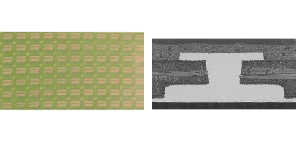
Substrate is made by single side build-up flow.
Applications
- Application Processor
- Networking
- Connectivity
Features
- Cost reduction
- Low profile
- Cost effective solution