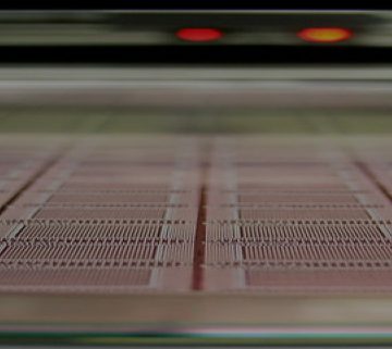
Heterogeneous Integration (HI)
The semiconductor industry is facing a new era in which device scaling and cost reduction will no longer continue on the path followed for the past few decades. Packing more transistors on a monolithic IC is becoming more difficult and expensive at each node. Semiconductor companies are now looking for technology solutions to bridge the gap and improve cost-performance, while at the same time adding more functionality through integration. Integrating all the functions into a single chip, known as system on a chip (SoC), presents many challenges that include higher costs and design complexities. An attractive alternative is heterogeneous integration that uses advanced packaging technology to integrate devices which could be separately designed and manufactured by the most suitable process technology in the most optimized way.
What is Heterogeneous Integration (HI)?
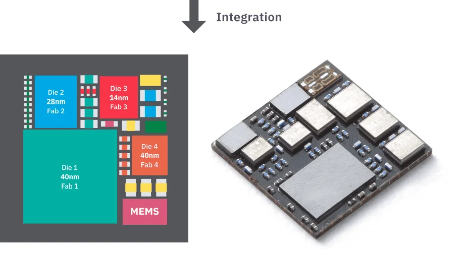
Heterogeneous Integration refers to the integration of separately manufactured components into a higher level assembly (System-in-Package, SiP) that, in the aggregate, provides enhanced functionality and improved operating characteristics. Source: Heterogeneous Integration Roadmap 2019 Edition CHAPTER 1 OVERVIEW.
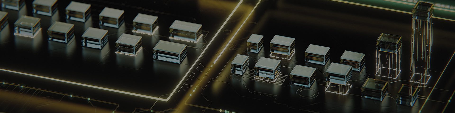
The combined components can vary in system level (e.g., pre-assembled package or subsystem), functionality (e.g., specialized processors, DRAM , flash memory, surface mount device (SMD), resistor/capacitor/inductor, filters, connectors, MEMS device, sensors) and technologies (e.g., one optimized for die size with another one optimized for low power). The overall idea behind heterogeneous integration is to integrate multiple dies in the same package. This enables the package to perform a specific and advanced function in a small form factor.

Advantages of Applying Heterogeneous Integration
Conventionally, the semiconductor industry tried to squeeze everything into one monolithic chip. However, it’s getting so expensive and the chip is getting so big. Heterogeneous integration tackles the age-old issue by combining chips with different process nodes and technologies. This technology enables the continued increase in functional density and decrease in cost per function required to maintain the progress in cost and performance for electronics. Heterogeneous Integration is essential to maintain the pace of progress with higher performance, lower latency, smaller size, lighter weight, lower power requirement per function, and lower cost.
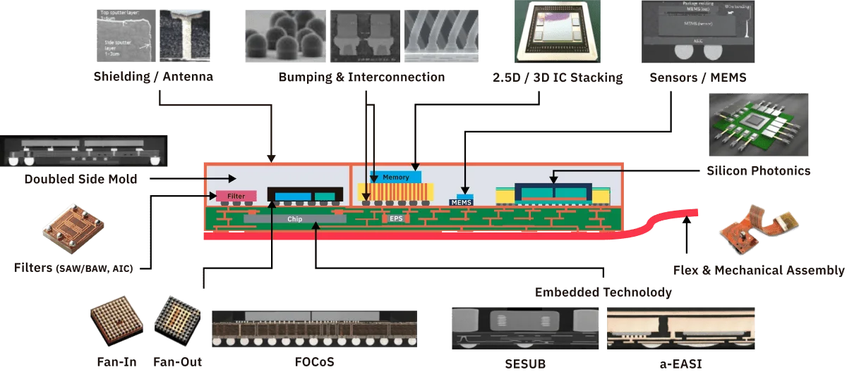
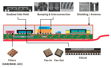
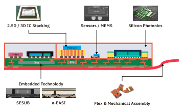
Technology Building Blocks for Heterogeneous Integration
Heterogeneous Integration Roadmap (HIR)
Emerging technologies—such as AI, 5G, edge, cloud, and data center, autonomous vehicles and wearable technology— hold great promise for improving the lives of individuals across the globe. The HIR maps out the future of system-level integration and the potential advanced packaging solutions necessary for implementing the emerging technologies.
ASE's Dr. William (Bill) Chen is leading the HIR initiative alongside Dr. Bill Bottoms of 3MTS (IEEE EPS), Tom Salmon (SEMI), S. Iyer (IEEE EDS), A. Helmy (IEEE Photonics), and Ravi Mahajan (ASME EPPD). The Heterogeneous Integration Roadmap is the result of dedicated collaboration and enormous effort by ASE contributors including Rich Rice, CP Hung, John Hunt and Mark Gerber, as well as the many contributors from across the electronics community. The 2021 edition of the Heterogeneous Integration Roadmap includes 24 chapters and can be downloaded by visiting https://eps.ieee.org/technology/heterogeneous-integration-roadmap/2021-edition.html.
Solution Platform
The ASE heterogeneous integration team possess many years of industry-leading experience in packaging and SiP technology development. ASE SiP technology enables ultra-compact, high-capacity, low-power module solutions with controller and sensor integration to meet the application needs of AI, IoT and mobile device miniaturization. The company has also developed various business models to actively promote the SiP eco-system. ASE’s innovative SiP and MEMS solutions leverage upon established IC assembly capabilities including copper wiring, flip chip packaging, wafer level packaging, fan-out wafer level packaging, 2.5D/3D IC and embedded chip packaging to address ongoing trends for the mobile device, IoT, high-performance computing, and IoV (Internet of Vehicles) markets.