Bumping Services
Wafer bumping is essential to flip chip or board level semiconductor packaging. Bumping is an advanced wafer level process technology where “bumps” or “balls” made of solder are formed on the wafers in a whole wafer form before the wafer is being diced into individual chips. Those “bumps”, which can be composed from eutectic, lead-free, high-lead materials, or Cu pillar on wafer are the fundamental interconnect components that will interconnect the die and the substrate together into a single package. These bumps not only provide a connected path between die and substrate, but also play an important role in the electrical, mechanical and thermal performance in the flip chip package.
Flip chip assembly package has traditionally been used for high-end niche applications. Recent technology development has adopted this process to be widely used in today’s consumer electronics applications. For the performance-driven market, flip chip interconnection reduces signal propagation delay, provide much better bandwidth, and relieves the constraints of power and ground distribution. For the form factor driven market, such as mobile applications, replacing wire bonding by flip chip interconnects reduces the size and weight of the package.
As the world leading IC assembly subcontractor, ASE established its wafer bumping services in 1999. Licensed from Flip Chip International, LLC, the world’s leader in printing bumping technologies, ASE’s flip chip bumping process has proven to be robust and reliable, with production experience accumulated since 2000 as the very first subcontractor to provide large volume production in bumping service.
ASE also established the plating bump process in 2003. The plating process has proven the robustness, reliability, and provided production service.
ASE's Wafer Bumping Capabilities
Currently, ASE operates state-of-the-art bumping facilities with varieties of bumping processes available for 200mm and 300mm wafer, all located in Kaohsiung, Taiwan. From 2017 to 2021, more than 5 million 8” wafers from over 60 customers’ devices as well as more than 5.3 million 12” wafers from over 110 customer’s devices have been processed in ASE’s plating and Cu Pillar bumping facilities with consistent 10% output growth per year. Since our fan-out platform began volume production in 2017, more than 1.1 million fan-out molding wafers had been produced until 2021.
Combined with other ASE manufacturing services including substrate design, substrate manufacturing, wafer sorting, bumping, backside grinding, backside marking, flip chip assembly, and final test, ASE offers customers unsurpassed flip chip as well as wafer level packaging turnkey solutions.
Advanced Bumping Technologies
ASE continues to invest in advanced technologies to maximize solutions for customers’ sophisticated chip designs. In collaboration with major integrated device manufacturers (IDMs) and the world’s top foundries, we’ve developed state-of-the-art wafer bumping capabilities including Polyimide Repassivation and RDL as well as 5nm/4nm Cu low-K wafer bumping.
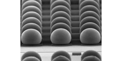
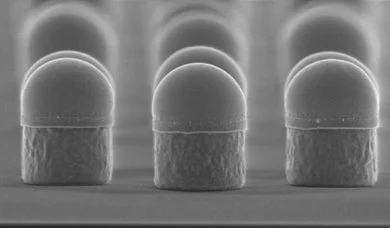
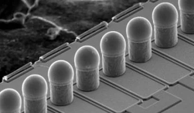
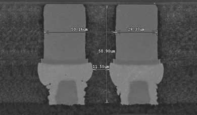
Cu Pilliar
As electronic devices trend further towards smaller, thinner, lighter, and higher performance characteristics, bump size likewise decreases meaning fine pitch becomes essential. ASE's Cu pillar bumps in flip chip packaging technology is the most effective method for fine-pitch interconnection for these package types.
Applications
Consumer
- Camcorders
- Digital Camera
- DVD
- WiMAX
Computer
- Voltage Regulators
- High-speed Memory
- Card
- PC Peripherals
Telecommunication
- Pagers
- Cellular Handsets
- GPS
Features
Standoff between chip and substrate is more stable. Good electrical performance and high reliability - Cu pillar bumps do not easily cause fatigue by electro migration and thermal. Fine pitch is possible below 45um. Cu pillar bumps do not cause bump bridging between adjacent bumps and they distribute current uniformly. Higher elastic modulus. Lower cost.