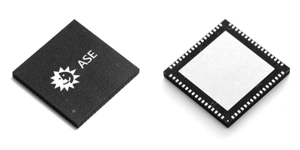
Based on copper lead frame, Quad Flat No-lead (QFN) or microchip carrier uses half-encapsulation technology to expose
the rear side of the die pad and the tiny fingers, which are used to connect the chip and bonding wire with the PCB. QFN
packages are suitable for applications over 12GHz working frequency. Providing both thermal and electrical enhancement,
QFN is a Cost-effective packaging solution due to its economical materials and simpler packaging process.
Applications
Telecommunication Products
- Cellular Phones
- Wireless LAN
Portable Products
- Personal Digital Assistants
- Digital Cameras
Low to Medium Lead Count Packages
Features
- Small footprint
- Cost-effective
- Low profile (< 0.9 0.2 L/F + 0.65 Mold)
- Better electrical performance
- Light weight
- Better power dissipation
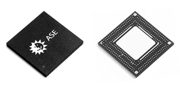
Advanced Quad Flat No-lead. aQFN™ is solution for Lead less, multi-row and fine-pitch lead frame package with
enhanced Thermal/ Electrical performance. aQFN™ is a Cost-effective packaging solution due to its economical materials
and simpler packaging process.
Applications
Telecommunication Products
- Cellular Phones
- Wireless LAN
Portable Products
- Personal Digital Assistants
- Digital Cameras
Low to Medium Lead Count Packages
Features
- Low profile, small footprint and light weight
- Excellent thermal performance
- Cost-effective package
- Free-form I/O design
- Excellent electrical performance
- Extend QFN I/O count up to 400
- Fine lead pitch 0.4mm
- Good SMT performance
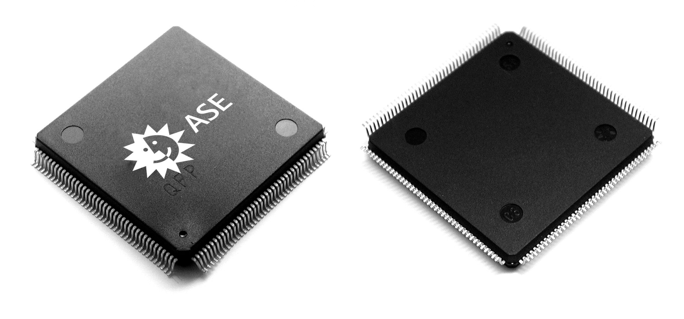
Quad Flat Package (QFP) is popular among the quad packages. The reason is the fine etching or stamping lead frames
enables QFP to contain more leads and feature a smaller profile to perform better electrical characteristics by
shortening the interconnection (the lead width can be as small as 0.16mm while the outer lead pitch is 0.4mm only). The
thinner and flexible leads in gull-wing shape also provide better 2nd-level reliability (package-to-PCB reliability).
The package with drop-in HS can allow more than 50% power dissipation compared with a conventional package (e.g. in
QFP 28x28mm, the allowable power of standard type and the type with HS is about 2.1W and 3.5W respectively). This
drop-in HS drives off the heat from the chip more easily by extending the conduction area, and transferring more heat
via the lead frame. QFP with drop-in HS is to package sizes of 14x20, 28x28, and 32x32mm.
Applications
Products
- Portable Consumer Products (PDA, Digital Camera, etc)
- System Board
- Power Controller
Quad packages have been used for years to meet increasing challenges of faster processors/controllers, ASICs, DSPs,
gate arrays, logic, memory ICs (EEPROM, Flash, DRAM & SRAM), PC chipset, video-DAC, multi-media and other related
application.
HS-QFP is suitable for use in high thermal applications like power & voltage regulators, power amplifiers, etc.
Features
- High-speed data processing
- MCM/stack structure design
- Pb-free process ready and available
- High-density interconnection
- High thermal conductive
- JEDEC standard compliant
- Cost competitive
- fine-pitch wire bond capability

Low profile and thin Quad Flat Packages (QFP) are classified by the overall thickness (t) according to JEDEC
definition:
- L type: 1.2< t <=1.7 mm
- T type: 1< t <=1.2 mm
Low profile and thin QFPs are becoming popular, as they are ideal for the applications in lightweight and portable
electronic products. ASE offers the lead count of LQFP/TQFP ranging from 32 to 256 and 44 to 176 respectively, covering
almost all the applications in memory, DSP, and communication ICs. Due to the low electrical parasitic out of the small
outline and shorter leads, low and thin QFPs are suitable for RFICs, and a Cost-effective alternative to expensive
ceramic QFPs.
Exposed Pad L(T)QFP
The exposed pad can be soldered to the PCB so that the heat can be driven off directly (the JA is only half as much
as the standard L(T)QFP). Besides, this pad is also electrically grounded, and thus results in far smaller ground
inductance. Exposed pad L(T)QFP is a Cost-effective solution suitable for enhancing thermal and electrical performance.
Applications
Telecommunication Products
- Cellular Phones
- Wireless LAN
Portable Products
- Personal Computer
- Personal Digital Assistants
- Digital Cameras
Low to Medium Lead Count Packages
Features
LQFP/EP-LQFP Packing Offering
- 7x7mm to 28x28mm body size available
- Wide selection of pad size to meet die requirements
- Customize leadframe design capability
- 32 ~ 256 leads counts available
- fine-pitch wire bond capability
- Lead free process ready and available
- High-conductivity copper leadframes
- Low-stress die attach materials
- Power enhancement version
- JEDEC standard compliant
TQFP/EP-TQFP Packing Offering
- 10x10mm to 20x20mm body size available
- Wide selection of pad size to meet die requirements
- Customize leadframe design capability
- 44 ~ 176 leads counts available
- fine-pitch wire bond capability
- Lead free process ready and available
- High-conductivity Copper leadframes
- Low-stress die attach materials
- Power enhancement version
- JEDEC standard compliant
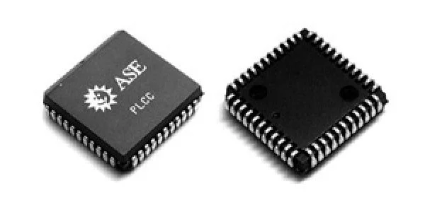
Plastic Leaded Chip Carrier (PLCC) is widely used in micro-controllers and consumer electronics. Each lead of the PLCC is formed into a "J"-shape and folded under the package body. ASE provides PLCC packaging services in compliance with JEDEC standard. Lead count ranges from 20 to 84 with 1.27mm (50mil) lead pitch.
Applications
ASE's PLCC product was designed in compliance with JEDEC standard for 'J' shape leaded SMT packages. Its robust leads and smaller foot space makes it applicable for surface mount and replaceable plug-in assembly via sockets.
Design applications include,
- Memory, Processors and Controllers
- ASIC, DSP, PC Chipset Device for Consumer Products, Automotive and Aerospace
Features
- 453~1153mils body sizes
- Wide selection of pad size to die size
- Pb-free process ready and available
- 28~84 available lead counts
- High-conductivity lead frame
- JEDEC standard compliant
- Wide selection of pad size to meet die size per customized lead frame design capability
Small Outline J-leaded (SOJ) package is similar to PDIP, but the leads' end are formed in a "J"-shape to be folded under the body. This aims to reduce the foot print. With the increasing popularity of SMT and with a smaller outline than PDIP, SOJ is widely used to complement PDIP.
Applications
Telecommunication Products
- Cellular Phones
- Wireless LAN
Portable Products
- Personal Digital Assistants
- Digital Cameras
- Audio/Video
Low to Medium Lead Count Packages
Features
- Low profiles and lightweight
- SOJ body sizes from 710 up to 1125 mils
- Existing BOM and process flow
- Steady yield
- Pb-free Process ready and available
- Low cost
- JEDEC standard outlines
The features of Small Outline Package (SOP) are similar to SOJ, except that the leads' end is formed in the shape of a gull-wing. Shrink small-outline package (SSOP) is the shrunk version of SOP, with lead pitch narrowed from 1.27mm (50mil) to 0.635mm (25mil). The shrunk body means flexible layout within finite PCB area. Another advantage is that shorter leads improve the electrical performance.
Applications
- Cellular Phones
- Digital Cameras
- Personal Digital Assistants
- Information Appliances
Features
- SOP body sizes 154 up to 450 mils
- SSOP lead counts available 48 & 56
- Pb-free process ready and available
- Pb-free process ready and available
- JEDEC standard outlines
- SOP lead counts available from 8 to 32
- Existing BOM and process flow
Plastic dual-in-line packaging (PDIP) is a principal package using the pin-through-hole (PTH) technology. It is widely used in low cost and manual applications. ASE offers PDIP with lead counts ranging from 8 to 64 leads and package width from 7.62mm (300mil) to 17.78mm (700mil). For package size reduction, ASE offers two alternatives - the narrow body type, Skinny PDIP (width is 300mil, lead count is 24, 28) and the narrow lead pitch type, Shrink PDIP or SDIP (lead pitch is 1.78mm or 70mil, lead count is 32, 56, 64).
Applications
Dual-in-line packages are considered one of the more established industry standard packages. PDIP’s broad ranges of applications include logic, memory ICs, microcontrollers, and logic, power ICs used in automotive devices, consumer and communications products.
Features
- 300mil body width: 8, 14, 16, 18, 20, 24, 28 available lead count
- 700mil body width: 64 available lead count
- Pb-free process ready and available
- 400mil body width: 32 available lead count
- EDEC standard compliant
- 600mil body width: 24, 28, 32, 40, 42, 48, 56 available lead count
- Wide choice of pad sizes to meet die size per customer’s lead frame design capability