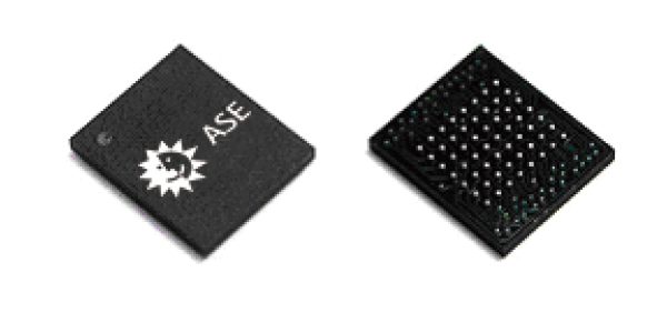
Wire Bond BGA

Ball-grid arrays (BGA) are IC packages, which place output pins in the form of a solder ball matrix. The traces of the BGA are generally fabricated on laminated substrates (BT-based) or polyimide-based films. Therefore, the entire area of substrates or films can be used to route the interconnection. BGA has the advantage of lower ground or power inductance thereby assigning ground or power nets via a shorter current path to PCB. Thermally enhanced mechanisms (heat sink, thermal balls, etc.) can be applied to BGA in order to reduce thermal resistance. The higher functional capabilities of the BGA package technology benefit high power and high speed ICs that require enhanced electrical and thermal performance.

Compared with traditional SMT packages, the advantages of BGA are as follows:

  • Higher interconnect density
  • Lower assembly cost
  • Self-alignment during reflow
  • Lower profile
  • Ease of thermal and electrical management
  • Ease of routing

ASE Wire Bond BGA Packaging Offerings

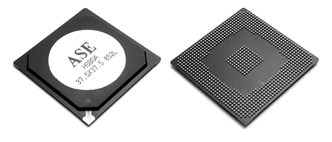
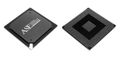
Plastic ball grid array (PBGA) are BGA packages adopting plastic (epoxy molding compound) as the encapsulation. According to JEDEC standard, PBGA has an overall thickness of over 1.7mm.

Applications

ASE PBGA's design and features improve the performance of

  • Graphics
  • PC Chipsets
  • Microprocessors/Controllers
  • PLDs
  • Communications
  • ASIC, Gate Arrays
  • DSPs
  • Networking
  • Memory Packages

Features

BGA is suitable for high power and high speed ICs requiring superb electrical and thermal enhancement.

  • 15x15mm to 45x45mm package
  • Low assembly cost
  • Ease of thermal and electrical management
  • JEDEC MS-034 standard outlines
  • 119 balls to 1520 ball count
  • Self-alignment during reflow
  • Ease of routing
  • Lead free process available
  • High interconnect density
  • Low profile
  • Good power dissipation
  • Full In-house design capability

Heat Slug BGA (HSBGA) is an upgraded type of PBGA. Within the molding area, a piece of copper heat slug is implanted. The heat slug is intended to lower the thermal resistance (θJA) of PBGA without change of material. The θJA of HSBGA is generally 20% lower than PBGA and achieves 5 to 6W of thermal dissipation under natural convection. This technology can be applied to any kind of die-up substrates (e.g. 2- or 4-layer BT, and metal core). HSBGA is an excellent solution for cost-effective high power package, high-speed ICs like graphics chips, communication and networking ICs.

Applications

HSBGA is excellent for products that require improved thermal performance such as high power packages for high speed ICs in personal computers, networking and graphic ICs, data communication, consumer ICs and in telecommunication applications.

Features

HSBGA is suitable for high power and high speed ICs requiring superb electrical and thermal enhancement.

  • 15x15mm to 45x45mm package available
  • Good electrical performance
  • JEDEC MS-034 standard outlines
  • Full electrical and thermal characterization capability
  • 120 balls to 1520 ball count available
  • Good thermal performance
  • Lead free process ready and available
  • Cost effective
  • Good power dissipation
  • Full In-house design capability

Fine pitch Ball Grid Array (FBGA) are BGA package that follows JEDEC standard package outline dimension for DRAM products. To meet high speed DRAM requirement, FBGA can be designed the shorter trace length to provide better electrical performance than that of TSOP. Not only better electrical performance, FBGA's smaller package size allows higher memory density on memory module than that of TSOP package.

Applications

  • Computer, Communication, and Consumer Devices
  • Computer, Communication, and Consumer Devices

Features

  • 10x10.5 to 11x13mm packages are available
  • Low profile
  • Good solder joint reliability
  • Good electrical and thermal performance
  • JEDEC MO-207J standard outlines conforming
  • Meet JEDEC drop test/TCT requirement
  • Low assembly and test cost solution
  • RoHS and Halogen free conforming