
MEMS and Sensor Packaging
Micro-Electro-Mechanical Systems (MEMS) and sensors contribute to the myriad semiconductor technologies that allow us to experience and interact with our surroundings in revolutionary new ways. MEMS devices consist of mechanical elements, sensing features and electronic circuits integrated onto a silicon substrate. The elements in MEMS gather information from the environment through the measurement of mechanical, thermal, biological, chemical, acoustic, optical and magnetic stimuli. Wafer level packaging and TSV technologies are key enabling packaging technologies that optimize size, functionality, performance as well as deliver cost-effective integration for MEMS packaging. ASE has extensive modeling lab capabilities, including optical lab simulation and measurement, as well as expertise in material measurement and stress simulation. These services are all areas of extreme importance to MEMS & Sensor manufacturing.
Introduction
MEMS and sensors serve as gears to connect people with their surroundings, and enable deeper perception and interaction to the environment. We are able to leverage the information that sensors perceive to develop functions that improve the quality of life. The rise in robotics, autonomous vehicles, smart homes, IoT, AR/VR/MR, and environmental hubs has become the driving force for the acceleration and development of MEMS and sensor technology.
 Different Types of Sensors
Inertial
- Gyroscope
- Accelerometer
- Magnetometer/Hall-Effect Sensor
- Combo & IMU
Light & Radiations
- X-ray Sensor
- Bolometer
- IR Sensor
- IR Thermopile
- UV Sensor
- PALS/ALS
- LiDAR
RF
- Oscillators
- Switches
- SAW Filters
- FBAR/BAW Filters
Environmental
- TPMS Module
- Gas Sensor
- Pressure Sensor
- Temperature Sensor
- Humidity Sensor
- Si Microphone
Others
- Optical/micromirror
- LED
- Ultrasonic Sensor
- Medical Sensor
What is MEMS and Sensors Packaging?
MEMS are a process technology used to create tiny integrated devices or systems that combine mechanical and electrical components. These devices have the ability to sense, control and actuate according to set parameters. While traditional packaging is used to protect chips, MEMS packaging is integral to the functionality of the device. Each sensor device has unique packaging requirements to meet specific functions for interacting with external devices or the environment. For example, speakers, microphones and pressure sensors must have sound or pressure inlets integrated using MEMS and sensor packaging techniques. Optical devices may require certain types of materials to be used so that the desired optical wavelengths may be detected. MEMS and sensor packages can be further differentiated into mold type, air type with leadframe/organic substrate/ceramic substrate and metal/plastic packages and wafer-level packaging, providing comprehensive solutions for sensor and device protection according to the type of application and the commercial/reliability requirements.
Advantages of MEMS and Sensors Packaging
The integration of MEMS sensors in chips are used in a diverse array of industries including automotive, consumer and industrial applications. MEMS and Sensor packaging offer advantages such as modularity, high flexibility and reasonably low fabrication complexity with integration of the integrated circuit and micromechanical components. Compared with conventional packaging processes, MEMS and sensor packaging are more application-dependent and provide several benefits that include:
Support optically compatible material
- Clear molding/encapsulation
- Customized dyed encapsulant
- Filter coating
- Silicon or plastic lens and Microlens array
Improve sensor function
- Optical simulation
- Hermetic sealing
- Dedicated assembly methodology
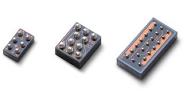
ASE MEMS and Sensors Packaging Offerings
ASE offers a variety of sensor packaging solutions that leverage upon an established database of material properties and assembly experience to address dedicated sensor requirements of different microelectronic, optoelectronic, RF, biomedical device, sensor, actuator and microsystem applications.
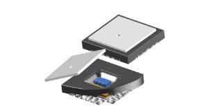
OCQFN
Pressure Sensor
- Pkg~ 7x7
- MEMS(accelerometer & pressure), MCU integration
- Since 2014
OCQFN (Open Cavity Quad Flat No-lead):
- Cost-efficient and mature packaging
- Also suitable for gas sensor, emitter/receiver
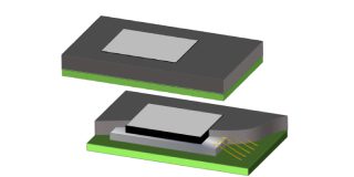
OQFN
Ambient Light Sensor
- Pkg~ 2x2
- Support consumer, automotive application
- Since 2016
OQFN (Optical Quad Flat No-lead):
- Transparent molding compound is available
- Also suitable for gesture sensor, emitter/receive
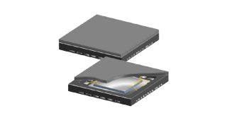
CoW
Timing
- Pkg~ 1.5x1
- MEMS oscillator
- Since 2017
CoW (Chip on Wafer):
- WLCSP
- Also suitable for silicon photonics, imaging sensor
OLGA
Proximity Sensor
- Pkg~ 2.5x1.5
- ALS, color, gesture integration
- Since 2015
OLGA (Optical Land Grid Array):
- Assembly of proprietary plastic panel
- Clear molding
- Customized molding lens
- Also suitable for bio sensor, ToF* sensor, imaging sensor
PMQFN
RFIC
- Pkg~ 5x5
- Molded fence with cover
- Automotive grade reliability
- Since 2015
PMQFN (Pre-mold Quad Flat No-lead):
- Semi-hermetic
- Also suitable for illuminator capable of fall-off detection, LiDAR receiver, emitter
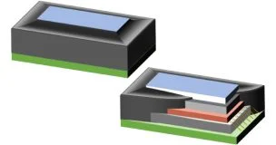
iLGA
Fingerprint Sensor
- Pkg~ 16x6
- Collimator integration
- Dispensed/Molded encapsulant
- Since 2016
iLGA (image Land Grid Array):
- Wafer-level collimator/lens
- Strip-level filter coating
- Also suitable for LiDAR imaging, CMOS image sensor
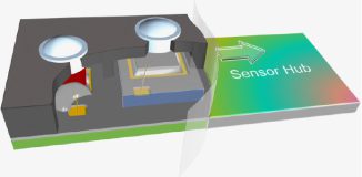
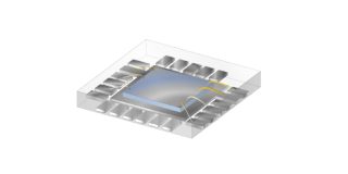
LiDAR Receiver Packaging Offerings
ASE offers advanced sensor solutions for the automotive industry, in particular the application of LiDAR (light detection and ranging) remote sensing technology in autonomous vehicles. LiDAR sensors measure distances and scan the environment with a high level of accuracy. Conventional LiDAR sensors can send out infrared light, and measure the time it takes for the light to bounce off an object and back to the sensor, creating a three-dimensional map. In addition to the spatial coordinates (distance), advanced LiDAR such as Frequency Modulated Continuous Wave (FMCW) LiDAR can further determine the reflectivity* and speed of the object (5D). The 3D or 5D maps provide information that allows autonomous vehicles to react promptly and take preventive measures in different traffic scenarios. Our packaging solutions support mechanically spinning LiDAR or solid-state LiDAR using avalanche photodiode (APD), single photon avalanche photodiode (SPAD) or silicon photomultiplier (SiPM).
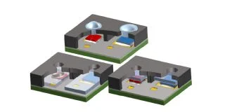
CoW LGA
CoW for compound semiconductor & CMOS ROIC integration, spacer for interference immune, glass sealing process, bandpass filter on glass, wire coating
QFN
Pre-mold flat lead-frame, plastic lid with glass cover, semi-hermetic sealing
OLGA
CoW for compound semiconductor & CMOS ROIC integration, double plastic lid for particle resistance, bandpass filter on glass
Key Growth for MEMS and Sensors Applications

Mobile/Consumer
- Smartphone
- Wearable device
- AR/VR/MR
- Medical & Biometrics

Industrial/Automotive
- Automotive
- ADAS & Autonomous system
- Robotics & Automation
- Industry 4.0

Communication
- High-Performance Computing
- 5G/IoT/Environmental hubs
- Artificial Intelligence & Machine Learning