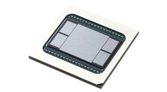
ASE has introduced VIPack™, an advanced packaging platform designed to enable vertically integrated package solutions. VIPack™ represents ASE’s next generation of 3D heterogeneous integration architecture that extends design rules and achieves ultra-high density and performance. The platform leverages advanced redistribution layer (RDL) processes, embedded integration, and 2.5D and 3D technologies to help customers achieve unprecedented innovation when integrating multiple chips within a single package.
As our world navigates the data-centric era, the semiconductor market is growing exponentially, with the growth behind the data coming from devices used across Artificial Intelligence (AI), Machine Learning (ML), 5G Communications, High-Performance Computing (HPC), Internet-of-Things (IoT), and Automotive applications. Demand for innovative package and IC co-design, cutting-edge wafer level fabrication processes, sophisticated packaging technologies, and comprehensive product and testing solutions has never been greater. The role of packaging has become increasingly critical, as applications call for solutions to enable higher performance, greater functionality, and improved power, while meeting stringent cost parameters. The rising adoption of chiplet-based co-designs is further fueling demand for multi-chip integration into a single package. The launch of VIPack™ firmly establishes a collaborative platform for exceptional interconnect solutions where 3D heterogeneous integration has become critical.
ASE’s VIPack™ is comprised of six core packaging technology pillars supported by a comprehensive and integrated co-design ecosystem:
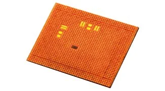 FOPoP
FOPoP
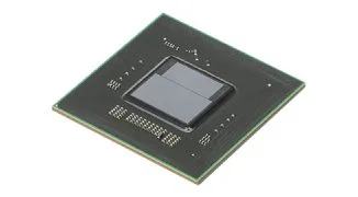 FOCoS
FOCoS
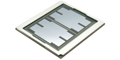 FOCoS-Bridge
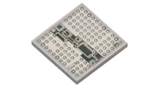 FOSiP
FOSiP
 2.5D/3D
 Co-Packaged Optics
These include ASE’s high density RDL-based Fanout Package-on Package (FOPoP), Fanout Chip-on-Substrate, (FOCoS), Fanout Chip-on-Substrate-Bridge (FOCoS-Bridge), and Fanout System-in-Package (FOSiP) as well as Through Silicon Via (TSV)-based 2.5D and 3D IC and Co-Packaged Optics processing capabilities. The VIPack™ platform provides the capabilities necessary to enable trailblazing highly integrated silicon packaging solutions required to optimize clock speed, bandwidth, and power delivery, and to reduce co-design time, product development, and time to market.
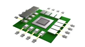
The VIPack™ platform delivers the dense horizontal and vertical interconnect solutions required to interconnect disaggregated SoCs (System-on-Chip) and HBM (High Bandwidth Memory) used for leading-edge HPC, AI, ML, and Network applications. High-speed networking is also being challenged with several complex components for optical packaging that require VIPack™ innovation to bring these components together in a vertical structure for both space and performance enablement. Applications supported by VIPack™ further extend to the mobile market with ultra-low profile SIP modules to address the common RF iterative design process and enable a higher level of performance with integrated passives in the RDL layers. Additionally, the next generation of application processors address the demand for lower profile package solutions, while solving power delivery issues for advanced silicon nodes.
Available now, ASE’s VIPack™ is a scalable platform that will expand in alignment with industry roadmaps.
Blog: Introducing VIPack™ by Mark Gerber