FOPoP
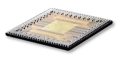
Today’s portable electronic products such as smart phones, versatile tablets, and wearable devices, require packaging innovation that enables greater functionality, better performance and smaller footprint, at a lower cost. Conventional interposer-based PoP (Package-on-Package), featuring via stacking of two or more packages on top of one another, integrates multiple functionalities while offering flexibility, improved cost, and faster time to market. To further reduce the package profile and improve electrical and thermal performance, a redistribution layer (RDL) based POP called fan-out package on package (FOPOP) has been introduced. ASE’s FOPoP lowers latency and delivers exceptional bandwidth advantages for the dynamic mobile and networking markets.
What is Fan-Out Package on Package (FOPoP)?
FOPoP, as one of the core packaging technology pillars in VIPack™ platform, is a RDL based package which combines a fan-out bottom package with a standard package mounted on the top side and utilizes fine pitch plated Cu posts for through-mold vertical interconnections. The bottom package has two RDLs (top and bottom routing planes) connected by the Cu posts, which are formed by a wafer-level fan-out technology which enables thinner and finer electrical traces.

Fan-Out Package on Package (FOPoP)
Fabrication Process of FOPoP
The FOPoP fabrication process is similar to conventional PoP process except that the bottom package is formed by a RDL-first fan-out process mainly including the following steps:
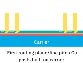

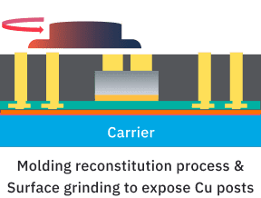
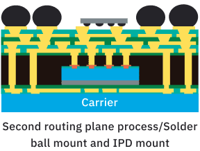
Note that the copper posts are plated onto the temporary carrier prior to die attach, and the second routing plane is connected to the copper posts exposed from the molding material by grinding.
Benefits of FOPoP
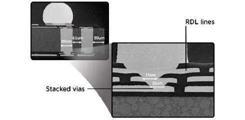
Compared with conventional interposer-based PoP, FOPOP has a thinner profile and better electrical and thermal performances since the bottom package eliminates the need for an interposer. By using PoP technology, the KGD issue can be mitigated since the top package can be burn-in and tested before mounting to the bottom package. The development cycle time and cost can also be reduced since top and bottom packages can be decoupled from each other from the perspective of qualification, yield, sourcing, procurement timing and logistic handling. In addition, new interconnect capabilities, proximity-driven impedance enhancements, stacked vias, and vertical coupling enablement are amongst key drivers in the new vertical integration methodology used with the FOPoP structure.
For mobile applications, the fundamental high-density, substrate-less configuration of the FOPoP package results in exceptional package performance, due to elimination of the substrate parasitic inductance along with a thinner package form factor. Overall, the FOPoP structure provides higher interconnection density and integration through a finer line space RDL, a shorter interconnect length resulting in better electrical performance, and a smaller, thinner form factor. The FOPoP package platform is enhanced for increasing complexity and high-performance needs by enabling RDL on both sides of the die for increased integration and functionality. Furthermore, both landside caps and near-die deep trench capacitors can be implemented to meet the power integrity requirements of advanced nodes.
For networking applications, FOPoP helps to enable the next generation of bandwidth from 400G to 800G pluggable optical transceivers, while also presenting a highly viable integration solution for Co-packaged Optical (CPO). 3D stacking provides much shorter interconnection between the photonic integrated circuit (PIC) and controller to reach much higher speed. Small form factor SiPh engines become easier to package with an ASIC because FOPoP 3D stacking is a higher bandwidth per size solution, which is the key enablement of CPO.
Key FOPoP benefits for the mobile market:
- Ultra-low profile achieves almost 40% reduction in height over substrate-based package-on-package structures.
- Improved electrical efficiencies deliver power benefits for advanced silicon nodes.
- Advanced materials that enable good warpage results at high temperature allow for good surface mount yields.
- Stable Dielectric Constant (Dk) over wide high frequency range with a reduced material response when using Fan Out Polyimide vs. traditional substrate-based dielectrics.
- New processes and structures will allow for an expanded roadmap that will enable both heterogeneous and homogeneous integration of chiplets in the future.
Key FOPoP benefits for the networking market:
- Reduces electrical path by 3x and enables a denser bandwidth by up to 8x, allowing engine bandwidth expansion up to 6.4 Tbps per unit.
- Improves energy efficiencies from 25pJ/bit to 5pJ/bit.
- Controls losses above 10GHz frequency range
- Offers the most advanced integration of PIC, controller chips, and special pre-alignment structure for laser, optics, and fiber array units.
- Provides sub-µm accuracy and improves optical coupling performance as well as assembly efficiency by using passive alignment.
FOPoP Applications
FOPOP has become a promising 3D integration solution for the application processor (AP) and memory combination, application-specific integrated circuit (ASIC) and antenna-in-package combination, as well as electronic integrated circuit (EIC) and photonic IC (PIC) combination.

AP + Memory (4G/5G)

ASIC + Antenna (5G)

EIC + PIC (Networking)
FOPoP addresses complex architectural and integration requirements that help enable next generation solutions for application processors, mobile, automotive, antenna in package and co-packaged silicon photonics applications. In addition, FOPoP delivers exceptional performance advantages for augmented reality (AR), virtual reality (VR), mixed reality (MR), and networking applications, where size is paramount for improving the aesthetic form factor, increasing battery space, and achieving power savings through more efficient routing connections.


