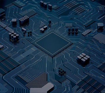
Silicon Photonics
AI is drastically changing the world, but creating unprecedented data levels and intensifying the critical need for energy efficiency. Hardware innovation is in the spotlight, with demand growing for reinvented data center infrastructure that enables accelerated compute and reduces power consumption while optimizing performance and lowering latency. Silicon photonics has emerged as a powerful technology, poised to revolutionize AI infrastructure by shifting from copper to light-based data transmission. Co-packaged optics (CPO) is a packaging technology that integrates optical components in the most innovative ways. ASE has demonstrated CPO technology that improves energy efficiency and scalability for AI applications.
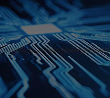
CPO PRESS RELEASE CPO BLOGSilicon Photonics (SiPh) and its Advantages
Silicon photonics (SiPh) serves as a medium for light transmission. Leveraging advanced semiconductor technologies, SiPh integrates seamlessly with the existing complementary metal oxide semiconductor (CMOS) ecosystem, encompassing both front-end and back-end processes. This enables the development of high-density photonic integrated circuits (PIC) that deliver complex optical functionality, such as filtering and modulation, on a compact, cost-effective chip. Compared to conventional electrical integrated circuits, which experience significant signal integrity challenges at high speeds, SiPh offers data transmission with higher bandwidth and greater energy efficiency.
The Evolution of Fiber Optics Integration
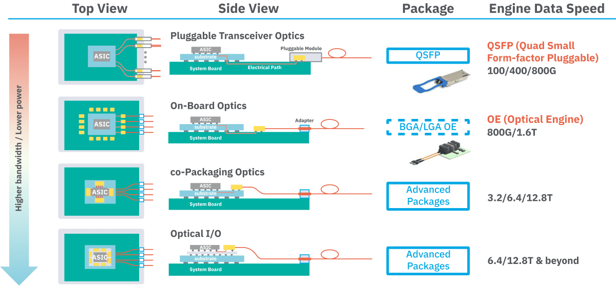
There are already silicon photonics based pluggable optical transceivers up to 800Gbps in commercial. Different with front-panel transceiver, optical engine can be populated around ASIC IC package as so-called on-board optics (OBO), which is able to support 1.6T Gbps. Additional to OBO, “Co-packaged Optics” and “Optical I/O” is promising to further shorten electrical paths with highly assembly integration, so that it is possible to deliver even higher bandwidth to ensure better energy efficiency (pJ/bit) and capital expenditure ($/Gbps) over pluggable optics.
Silicon Photonics Technical Building Blocks
Unlike common semiconductor manufacturing experiences, silicon photonics products may need more attentive consideration when defining the overall process flow to address optical performance.
Here, we list key technologies to enable pluggable, on-board and co-packaged optics:
- Post-fab wafer-level bumping and Si-etch process
- High-accuracy laser die bonding
- Advanced 2.5D/3D packaging (TSV/FO/CoW) for EIC*/PIC die integration
- Wafer-level optical probing test for known good SiPh PIC die
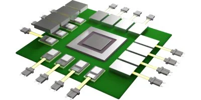
- Optical component assembly evaluation for future OBO*/CPO* application
- MCM module assembly
SiPh Based Pluggable Module Manufacturing Flow


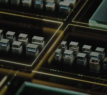
Silicon Photonics Applications
Silicon photonics enables heterogeneous on-board optics, co-packaged optics and optical I/O packaging, which is promising to realize the following applications.
- Hyperscale Data Center
- High-Performance Computing (HPC)
- Artificial intelligence & Machine learning (AI & ML)