Blog
Enabling Next-generation System Integration with Scalable SiP Solutions for Healthcare Applications
Evelyn Lu
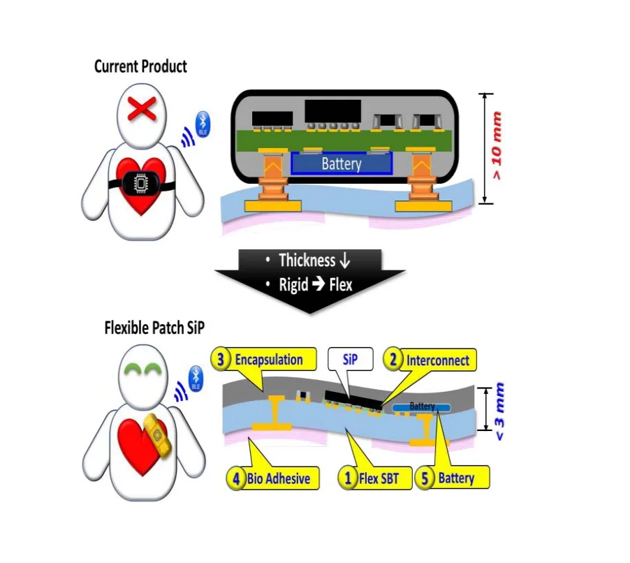
Semiconductor miniaturization and chip integration trends are driving greater industry focus on system-in-package (SiP) developments. SiP is a cost effective package integration technology that features higher performance and reduces time to market. These advantages allow chip companies to design electronic products that integrate more functions and develop new technology applications. Dr CP Hung, vice president, ASE Corporate R&D offers an insight on the application of SiP technology in healthcare electronics.
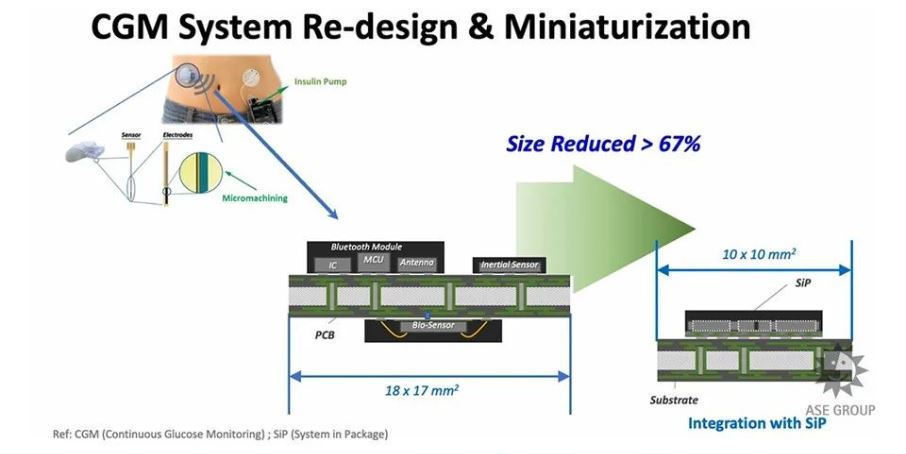
Continuous Glucose Monitor
A continuous glucose monitor (CGM) is a small wearable device that tracks blood sugar levels throughout the day and help detects trends and patterns. The data allows doctors and patients to better manage diabetic conditions. A CGM consists of a sensor, data transmitter and receiver, and the results are tracked via a monitor or a smartphone app.
ASE’s SiP technology supports the integration of different microcontrollers (MCUs), application-specific integrated circuits (ASICs), antennas and sensors that control all the functions in a CGM, onto a single package structure. The packaging process offers miniaturization without compromising the performance of the device.
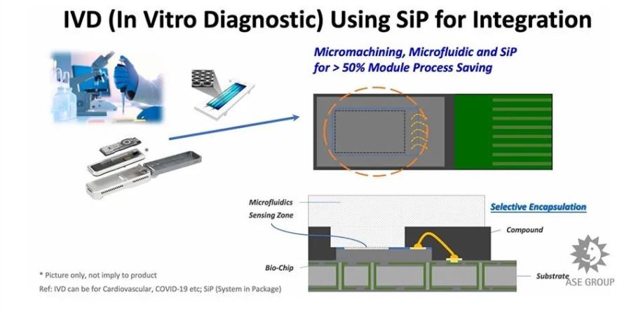
In Vitro Diagnostics
In vitro diagnostics (IVD) are tests performed on samples, such as mucus or blood, taken from the human body to help detect diseases or other conditions. The information obtained from analysis of such samples are used by health practitioners to monitor a patient’s overall health, and to treat or prevent diseases. A variety of IVD devices and systems are used by healthcare professionals in clinics, labs and hospitals, as well as by consumers at home.
Complex IVD module designs are made possible with SiP technology processes that allow the integration of the bio-sensor chips and the microfluid receptacle through the use of customized molding techniques.
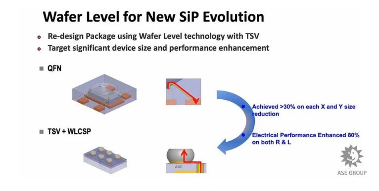
Sensor Applications
Wafer-level SiP technology is another packaging technique that applies through-silicon via (TSV) chip-scale package (CSP) processes to reduce the XY area size by 30% compared with traditional quad flat no-lead (QFN) packaging. At the same time, the electrical performance of the package structure is enhanced through lowering the resistance level by almost 80%.
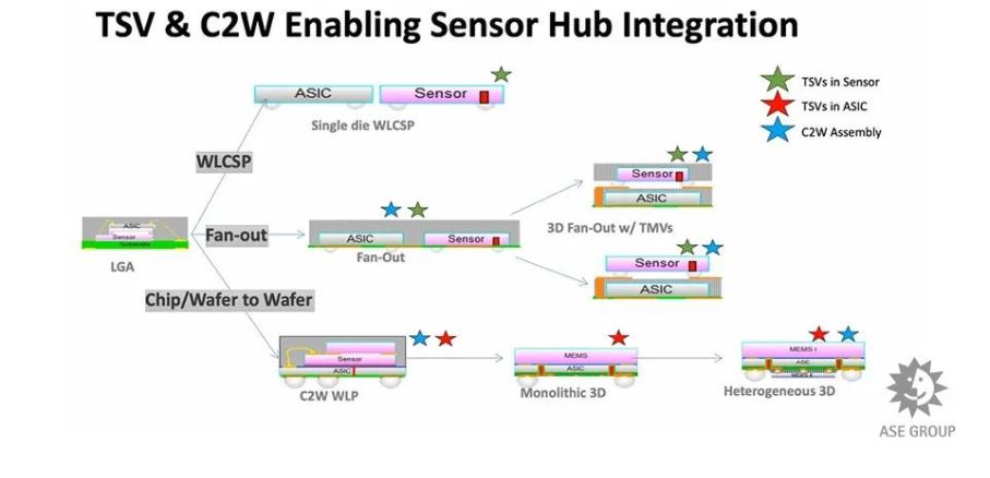
Sensor Hub
A sensor hub is a microcontroller unit that integrates and processes data from various sensors. Through-silicon via (TSV) and chip-to-wafer (C2W) bonding are techniques used to design chips inside sensor hubs. Other methodology of chip design include placing ASIC and sensor components side-by-side, or placing a TSV die on top of another standard die.
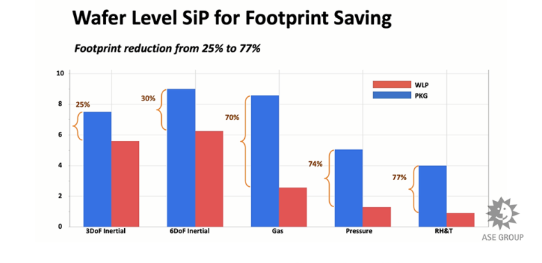
Wafer-level SiP technology can be applied in many types of sensor packages including 3D inertial, gas, temperature and humidity sensors. The data in the diagram shows that WL SiP package sizes can be reduced by between 25% to 77% compared with traditional packaging processes.
ASE provides a complete suite of packaging and test services – from package design, functional simulation to testing, verification, volume production and final testing. ASE continues to provide industry-leading system-in-package integration solutions to help customers speed up product development.