Electrical Lab
The ASE Electrical Laboratory (E-Lab) is dedicated to providing IC package electrical characteristics design, analysis and characterization in terms of simulation and measurement techniques. ASE E-Lab works closely with customers for the IC package design optimization, system-level SI/PI analysis, high speed/ frequency performance verification, and turnkey passive filter solutions. ASE E-Lab also provides customers the advanced and accuracy measurement service for the package characterization, electrical failure analysis, and both chip and system level mmWave antenna-in-package (AiP).
Design Service
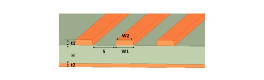
- Impedance
- Package Design Optimization (DDR, SerDes, Power, ….)
- RF Filter Design and Characterization
- Package EMI Shielding Design (Conformal and Compartment)

Modeling Service
- Package R/L/C Modeling
- S-parameter Modeling
- Package IBIS/SPICE/S-param. Model Export
SI/PI Service
Signal Integrity Analysis
- TDR Simulation
- Eye Diagram
- Crosstalk/Jitter/Timing Analysis
Power Integrity Analysis
- DCIR Drop
- PDN
- De-Cap Optimization
- Power Noise
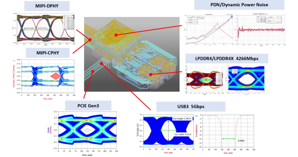
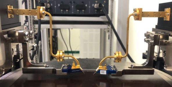
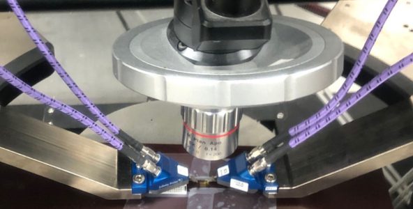
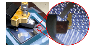
S-parameter
- Up to 170 GHz, Double-side S-parameter Probe Station
- Up to 260GHz, Single-side S-parameter Probe Station
- 12” Wafer and Panel-level Size S-parameter Probe Station
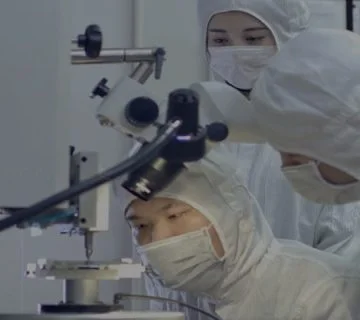
Electrical FA
- TDR Impedance
- 4-Wire DCR (Open/Short)
Parasitic
- Component level
- On-Chip Capacitor
- RF Inductor
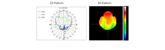
Spherical Chamber
- Chip/Package Level Passive Test with A Probing Feed
- Spherical & Direct Far Field
- Frequency: 18-110GHz
- Antenna Gain, 2D Pattern
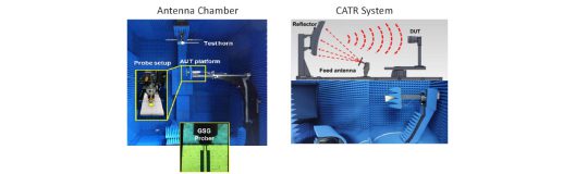
Compact Antenna Test Range (CATR) Chamber
- System Level Active Test with A Connector Feed
- Quiet Zone: 30x30 cm²
- Frequency: 18-110GHz
- Antenna Gain, EIRP, 3D Pattern
- Beamfroming Test