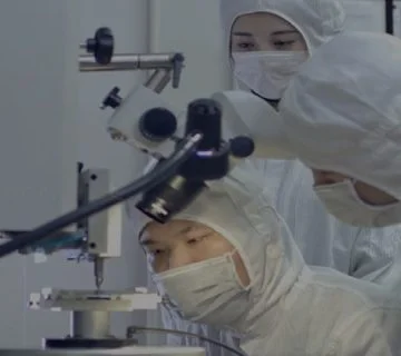
Stress and Thermal Lab
Modeling and Simulation
Stress-Thermal Laboratory provides package mechanical stress, thermal dissipation efficiency and mold flow phenomena analysis by numerical simulation report to customers for characterization evaluation. The analyses include package level such as die crack, delamination, and optimal design for low stress and high reliability; board-level stress analyses to predict the fatigue life of solder joints, like temperature-cycling-test (TCT), drop test, bending test, and other reliability tests. Besides, dissipating the heat effectively from the chip is a major challenge for engineers. ASE also provides services to conduct component-level and system-level thermal analyses.
The modeling and simulation service include:
- Thermal stress analysis (warpage, die stress, delamination)
- System/board level analysis (TCT, drop, bending)
- Wirebonding/wire looping simulation
- Customized heat sink effects
- Preliminary thermal studies for MCM/SiP
- Hot spots impact evaluations
- Transient analyses for power pulse impacts
- Compact thermal models (CTMs) for system-level simulations
- Simulations for packages in sockets (burn-in/HTOL test conditions)
- Mold flow prediction
Go to ASE eService to request electrical modeling and simulation service.
Measurement
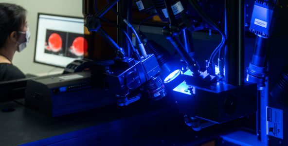
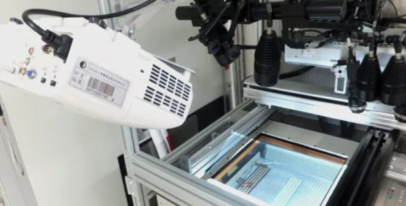
Stress-Thermal Laboratory provides mechanical and thermal measurement services to verify the package and system stress and thermal dissipation performance after the package designed and manufactured. In additional to package level measurements, we also support customers on chip level or board level measurements.
The measurement services include:
- Die strength flexural measurement
- Wafer/panel level warpage measurement
- Stud pull interface strength test
- Material dog bone tensile measurement
- Board/System level free fall measurement
- Die pull measurement (evaluate UBM/bump structural integrity)
- IC static force compression test
- Solder ball HBP (hot bump pull) strength test
- JEDEC/customized board level reliability measurement (TCT, THD, drop, shock, bending, vibration, twist)
Besides, thermal measurements include the measurements for package thermal parameters and material thermal conductivities:
- θJA (junction-to-ambient thermal resistance)
- θJB (junction-to-board thermal resistance)
- ΨJB (junction-to-board thermal characterization parameter)
- Wind tunnel testing (Integrated circuit thermal test with forced convection)
- θJC (junction-to-case thermal resistance)
- ΨJT (junction-to-top thermal characterization parameter)
- Material thermal conductivity measurements
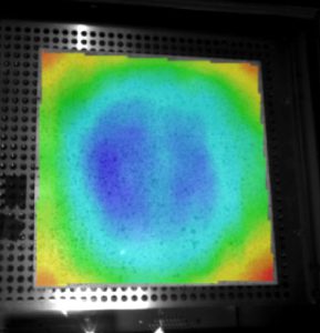
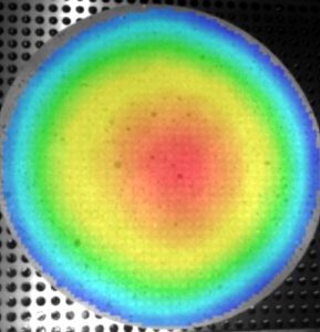
- IC hot spot analysis with thermal image
Package/System Design and Analysis
Base on long term experience and large database of package board level reliability, simulation, measurement and co-design projects with customers, ASE Stress-Thermal Laboratory developed package and system design capabilities to provide customers the pre-design solution. Package/System design and analysis service includes:
Package/System design and analysis service includes:
- Warpage & component stress prediction
- Package/board level reliability analysis
- Customized co-design/simulation (system analysis and co-design)
- Packaging material selection & structure design
- Thermal optimal design for packages