
Press Room
ASE K13 Groundbreaking Ceremony: Building a Complete Advanced Semiconductor Industry Cluster
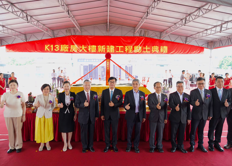
KAOHSIUNG, Taiwan, August 17, 2020 – Advanced Semiconductor Engineering, Inc. (ASE) hosted a groundbreaking ceremony for its K13 facility today, at the Nantze Export Processing Zone I. Key officials and VIPs including Ms Wang Mei-Hua, Minister of Economic Affairs; Mr Huang Wen-Guu, Director General of the Export Processing Zone Administration; Mr Chen Chi-Mai, Mayor-elect of Kaohsiung and Ms Liu Shyh-fang, Member of the Legislative Yuan were invited to witness another significant milestone set by ASE.
The rapid progress in 5G development has boosted demand for semiconductors, and to meet the explosive industry growth, major semiconductor players have continuously deployed investments. ASE is riding this industry trend by accelerating the process of smart manufacturing and expanding the scale of advanced manufacturing and production capacity. ASE will invest an initial NTD8 billion in the construction of the K13 facility, scheduled to be completed in 2023. The company will invest another NTD18 billion to expand manufacturing capacity for advanced packaging. Upon completion, ASE K13 is estimated to generate USD500 million annual revenue at full capacity. The facility will further create 2,800 jobs including the recruitment of semiconductor professionals that will help to strengthen Taiwan’s semiconductor industry leadership in the 5G market.
“Taiwan’s semiconductor supply chain plays a pivotal role in the global electronics industry with its unique advantages in the division of specialized labor and cluster effect. As the world’s leading packaging and testing company, ASE’s investment in NEPZ today will expand local employment opportunities and promote industry competitiveness. MOEA will also continue to invest in industrial intelligence, digital transformation and innovative applications, so as to build a complete semiconductor eco-system and to demonstrate government support for the domestic materials and equipment industry.”
– Ms Wang Mei-Hua, Minister of Economic Affairs, Ministry of Economic Affairs (MOEA)
“The Nantze Export Processing Zone (NEPZ) was established over 50 years ago and has now become a major location for global semiconductor packaging and testing thanks to ASE’s decision to establish its roots here and to continuously invest in Taiwan. In 2019, we launched the ‘NEPZ Diamond Field Renewal Project’, which is the largest joint investment project to date since NEPZ’s establishment. The project is supported by companies including ASE, Thinking Electronic Industrial Co, Orient Semiconductor Electronics and Hung Ching Construction, and aims to promote the transformation of the NEPZ into a high-tech smart industry zone, drawing more investments and creating more local employment opportunities.”
– Mr Huang Wen-Guu, Director General, Export Processing Zone Administration
“The US-China trade war has had a major effect on the semiconductor industry, with the world facing a supply chain transformation. Our future plans will be to position Kaohsiung as the ‘Asian High-end Manufacturing Center’ and ‘Advanced Semiconductor Manufacturing Center’. The establishment of the Chiaotou Science Park aims to attract more international corporations and in conjunction with the southern technology corridor, will elevate Southern Taiwan to be the world’s most important advanced semiconductor industry cluster.”
– Mr Chen Chi-Mai, Mayor-elect, Kaohsiung
“ASE is a global leader in the semiconductor packaging and testing industry, upholding a positive outlook, promoting sustainability development as its business goal, and playing an important role as an industry pioneer. The company is also simultaneously developing cutting edge technology, carrying out environmental conservation efforts, and focusing on people to create a positive workplace environment and corporate culture. I believe that ASE’s investment will develop better services for customers and partners, and enable Taiwan to continue to shine brightly in the industry.”
– Ms Liu Shyh-fang, Member of the Legislative Yuan
“As ASE continues to expand the scale of investment, we are seeking more R&D talents to join us and actively participate in the economic development of Kaohsiung. The K13 facility is constructed based on the trinity design concept of ‘smart technology, green energy and environmental protection, and employee care’. Advanced packaging technology will be the core focus of the facility. The development of a complete solution for a 5G+AIoT smart factory connected through high speed networks will enable us to achieve zero defects and higher efficiency in a real time manner.
The adoption of green construction methods that emphasize ecological balance, conservation, resource recycling and reuse, and green belts, demonstrate ASE’s commitment to sustainable development and environmental protection.
5G is the next evolution in technology that will boost business opportunities significantly. ASE will continue its investments in advanced manufacturing, integrate R&D and technology talents in Kaohsiung, seize opportunities for the future, and exert its influence in the global semiconductor industry.”
– Dr Tien Wu, Chief Executive Officer, ASE
The construction of K13 at NEPZ (I) is part of ASE’s ‘6 factories in 5 years’ investment plan, and an extension of the smart innovation model at NEPZ (II). Together with the investment in the K18 advanced packaging factory under the auspices of the ‘NEPZ Diamond Field Renewal Project’, ASE remains at the forefront in strategic deployment and is committed to build a complete semiconductor industry cluster in Kaohsiung that will drive the peak of production capacity.
K13 is designed with 2 floors underground and 12 floors above ground, with a total area of over 32,000 square meters. In addition to incorporating green building concepts of energy saving and environmental protection, the design also takes into account the needs of employees to create a comfortable and friendly workplace environment.
About ASE, Inc.
Advanced Semiconductor Engineering, Inc. (ASE), a member of ASE Technology Holding Co., Ltd. (NYSE: ASX, TAIEX: 3711) is the leading global provider of semiconductor manufacturing services in assembly and test. Alongside a broad portfolio of established assembly and test technologies, ASE is also delivering innovative VIPack™, advanced packaging, and system-in-package solutions to meet growth momentum across a broad range of end markets, including AI, automotive, 5G, high-performance computing, and more. To learn about our advances in SiP, fanout, MEMS and sensor, flip chip, and 2.5D, 3D and TSV technologies, all ultimately geared towards applications to improve lifestyle and efficiency, please visit: ASE Website , or follow us on LinkedIn & X: @aseglobal.