Press Room
ASE drives latency and bandwidth innovation with VIPack™ Fanout Package-on-Package
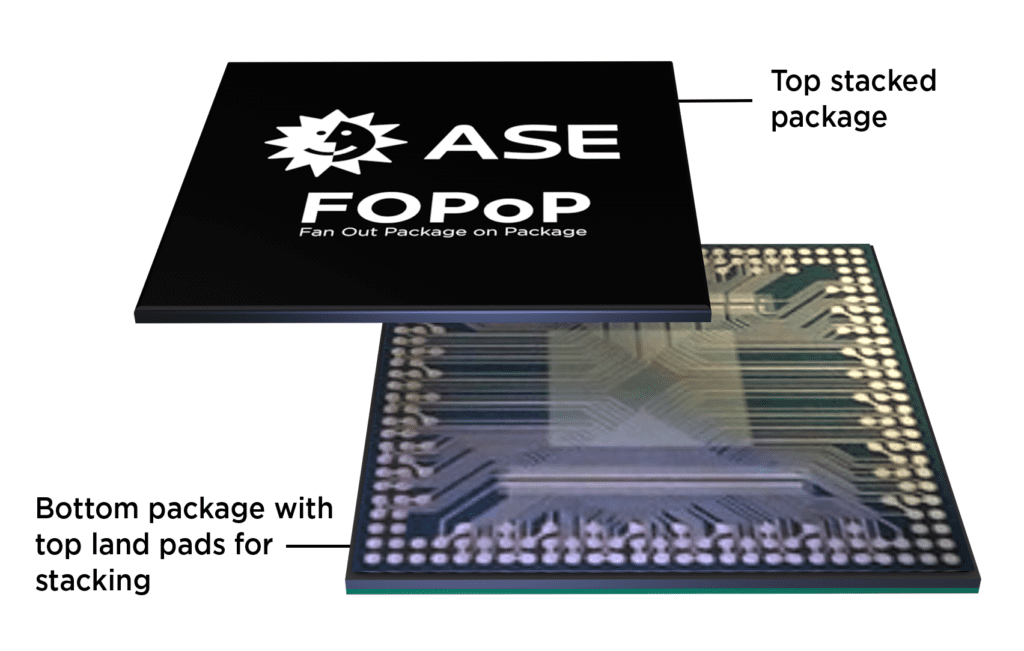
SUNNYVALE, Calif., Mar 14, 2023 – Advanced Semiconductor Engineering, Inc. (ASE), a member of ASE Technology Holding Co., Ltd. (NYSE: ASX, TAIEX: 3711), today announced its most advanced Fan-Out-Package-on-Package (FOPoP) solution, developed to lower latency and deliver exceptional bandwidth advantages for the dynamic mobile and networking markets. Positioned under the ASE VIPack™ platform, FOPoP reduces the electrical path by 3x and enables bandwidth density by up to 8x, allowing engine bandwidth expansion up to 6.4 Tbps per unit. FOPoP is a prominent package pillar addressing complex architectural and integration requirements that help enable next generation solutions for application processors, antenna-in-package devices, and silicon photonics (SiPh) applications.


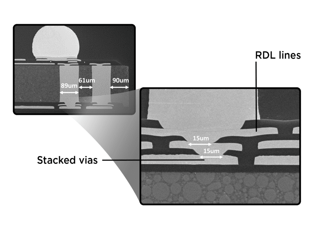
Today’s competitive markets are placing unprecedented reliance on the performance advantages achieved through advanced packaging innovation. In particular, expanded form factor and electrical benefits support customers as they transform their products to connect more people and things, more efficiently than ever. With 5G in the mainstream, there is growing demand for sophisticated applications that rely on ultra-low latency, particularly in instances where speed and efficiency can prove both life-enabling and lifesaving. ASE’s FOPoP structure leverages the most advanced integration technologies that extend long term roadmap requirements. New interconnect capabilities, proximity driven impedance enhancements, stacked vias, and vertical coupling enablement are amongst key drivers in the new vertical integration methodology used with the FOPoP structure.
For mobile applications, the fundamental high-density, substrate-less configuration of the FOPoP package results in exceptional package performance, due to elimination of the substrate parasitic inductance along with a thinner package form factor. Overall, the FOPoP structure provides higher interconnection density and integration through a finer line space RDL, a shorter interconnect length resulting in better electrical performance, and a smaller, thinner form factor. The FOPoP package platform is enhanced for increasing complexity and high-performance needs by enabling RDL on both sides of the die for increased integration and functionality. Furthermore, both landside caps and near-die deep trench capacitors can be implemented to meet the power integrity requirements of advanced nodes.
For networking applications, FOPoP helps to enable the next generation of bandwidth from 400G to 800G pluggable optical transceivers, while also presenting a highly viable integration solution for CPO. 3D stacking provides much shorter interconnection between the photonic integrated circuit (PIC) and controller to reach much higher speed. Small form factor SiPh engines become easier to package with an ASIC because FOPoP 3D stacking is a higher bandwidth per size solution, which is the key enablement of CPO.
Key FOPoP benefits for the mobile market:
- Ultra-low profile achieves almost 40% reduction in height over substrate-based package-on-package structures.
- Improved electrical efficiencies delivers power benefits for advanced silicon nodes.
- Advanced materials that enable good warpage results at high temperature allow for good surface mount yields.
- Stable Dielectric Constant (Dk) over wide high frequency range with a reduced material response when using Fan Out Polyimide vs. traditional substrate-based dielectrics.
- New processes and structures will allow for an expanded roadmap that will enable both heterogeneous and homogeneous integration of chiplets in the future.
Key FOPoP benefits for the networking market:
- Reduces electrical path by 3x and enables a denser bandwidth by up to 8x, allowing engine bandwidth expansion up to 6.4 Tbps per unit.
- Improves energy efficiencies from 25pJ/bit to 5pJ/bit.
- Controls losses above 10GHz frequency range
- Offers the most advanced integration of PIC, controller chips, and special pre-alignment structure for laser, optics, and fiber array units.
- Provides sub-µm accuracy and improves optical coupling performance as well as assembly efficiency by using passive alignment.
“Over time, the mobile market has driven a reduced form factor for the application processor and memory combination, and this has traditionally utilized the PoP platform. The new enhancements around FOPoP are poised to benefit other application spaces, especially wearables such as AR/VR/MR, where size is paramount for improving the aesthetic form factor, increasing battery space, and achieving power savings through more efficient routing connections,” said Mark Gerber, Sr. Director of Engineering & Technical Marketing, ASE.
“FOPoP is proving its tremendous value within the mobile and networking arenas, two important areas where both conquering geometrical complexity and achieving electrical efficiency can literally be game-changing,” said Dr. C.P. Hung, Vice President of R&D, ASE. He added, “With our extensive experience and technical knowledge, combined with resolute commitment to research and development, ASE continues to innovate industry-leading packaging solutions that scale with customer demands.”
“Our VIPack™ platform momentum continues to accelerate through the laser-focused creativity at the core of our vertical integration technology strategy that ultimately ensures ASE delivers compelling solutions across multiple trending markets,” commented Yin Chang, ASE’s Senior Vice President of Sales & Marketing. He continued, “FOPoP is a prime example of the packaging ingenuity that is pivotal to helping our customers stay ahead of the curve and bring next generation capabilities to market.”
ASE’s FOPoP technologies feature within VIPack™, a scalable platform that is expanding in alignment with industry roadmaps.
Supporting resources
- For more about FOPoP, please visit: https://ase.aseglobal.com/en/technology/fopop
- For more about VIPack™, please visit: ase.aseglobal.com/en/VIPack
- Follow us on our LinkedIn page for targeted updates and announcements @aseglobal
- Follow us on Twitter @aseglobal
About ASE, Inc.
Advanced Semiconductor Engineering, Inc. (ASE), a member of ASE Technology Holding Co., Ltd. (NYSE: ASX, TAIEX: 3711) is the leading global provider of semiconductor manufacturing services in assembly and test. Alongside a broad portfolio of established assembly and test technologies, ASE is also delivering innovative VIPack™, advanced packaging, and system-in-package solutions to meet growth momentum across a broad range of end markets, including AI, automotive, 5G, high-performance computing, and more. To learn about our advances in SiP, fanout, MEMS and sensor, flip chip, and 2.5D, 3D and TSV technologies, all ultimately geared towards applications to improve lifestyle and efficiency, please visit: ASE Website , or follow us on LinkedIn & X: @aseglobal.