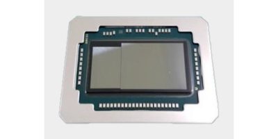
FOCoS
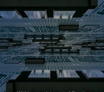
Chiplet integration* in high-performance computing (HPC) applications is high on the agenda these days, with escalating demand for reliable advanced packaging technologies to achieve critical interconnection as efficiently as possible. At ASE, our high-density FOCoS solutions offer that, and much more.
What is Fan-Out Chip on Substrate (FOCoS)?
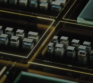
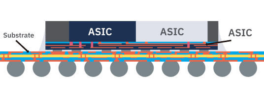
FOCoS is a fan-out package flip-chip mounted on a high pin count ball grid array (BGA) substrate. The fan-out package has a re-distribution layer (RDL) that allows the construction of shorter die-to-die (D2D) interconnections between multiple chips. The fan-out package is treated as if it was a single die and then flip-chip mounted onto the BGA substrate.
ASE FOCoS Package Offerings
FOCoS-CF (Chip First)
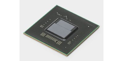
This FOCoS-CF test vehicle consists of two ASIC chiplets facing down directly connecting with RDL through the Cu vias and no micro-bumps between the Si dies and fanout RDL (L/S 2/2 um).
FOCoS-CL (Chip Last)
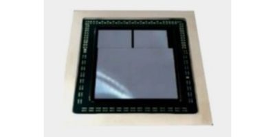
The FOCoS-CL test vehicle is built up by three chiplets (1 ASIC die and 2 HBMs) in a side-by-side configuration. The ASIC die and 2 HBMs are connected through RDL (L/S 2/2 um) and Cu micro-bumps.
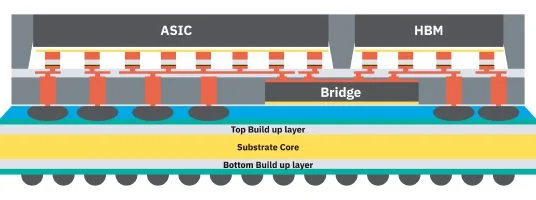
FOCoS-Bridge
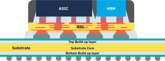
The FOCoS-Bridge test vehicle consists of 2 chiplets (1 ASIC die and 1 HBMs). The Si bridge die (L/S 0.6/0.6 um) are embedded in the fan-out RDL layer (L/S 10/10 um) for making the connection between ASIC and HBM.
Benefits of FOCoS
FOCoS eliminates the need for an interposer which helps to reduce the package cost. FOCoS also has less insertion loss, better impedance control and lower warpage, thereby offering better electrical performance.
Key Advantages of Applying Fan-Out Chip on Substrate (FOCoS):
- Lower cost (vs. 2.5D)
- Thinner package
- Good electrical performance (shorter D2D interconnects)
- High I/O counts (> 1000)
- Time to market with existing Fan-Out/Flip Chip techniques
FOCoS Applications
FOCoS is ideal for large package sizes and packages with high I/O density (> 1000 I/Os) that are designed for networking and server applications. The chip-last version of FOCoS can be used to package application-specific integrated circuits (ASICs) and high-bandwidth memories (HBM). Our various FOCoS solutions have provided a wide choice for chiplet integration in high-performance computing (HPC) and artificial intelligence (AI)/machine learning (ML) applications.
FOCoS Assembly Design Kit (ADK)
ASE, in collaboration with Siemens Digital Industries Software OSAT Alliance Program*, has developed a fully validated ADK that helps customers create and evaluate complex FOCOS packages in an easy-to-use, data-robust graphical environment prior to and during physical design implementation. By adopting the Siemens Xpedition Substrate Integrator and Calibre® 3DSTACK technologies, and through integration with the current ASE design flow, this ADK can significantly reduce FOCoS package planning and verification cycle times by about 30 to 50 percent in each design iteration. The comprehensive design flow enables us to quickly and easily co-design FOCoS packages with our customers and close any physical verification issues.
For more information about ASE’s ADK news, please visit https://ase.aseglobal.com/ch/press-room/high-density-advanced-package-designs-en/.