
Blog
Advanced Packaging Evolution: Chiplet and Silicon Photonics-CPO
Dr. Vincent Lin - Director, Corporate R&D
As we enter the AI era, the demand for enhanced connectivity in cloud services and AI computing continues to surge. With Moore’s Law slowing down, the increasing data rate requirements are surpassing the advancements of any single semiconductor technology. This shift underscores the importance of heterogeneous integration (HI) as a crucial solution for alleviating bandwidth bottlenecks. Today, OSAT (Outsourced Semiconductor Assembly and Test) is driven not only by the packaging demands of advanced node ICs but also by the rise of emerging technologies like Silicon Photonics and Co-Packaged Optics. ASE has introduced a Silicon Photonics packaging platform designed to deliver innovative solutions that facilitate more advanced AI systems while ensuring high performance and energy efficiency.
The Need for Improving Computing Performance while Enhancing Energy Efficiency
In the rapidly evolving world of artificial intelligence, the current training cycle hinges on three core processes: data collection, data connection, and leveraging High-Performance Computing (HPC) for AI training and inference.
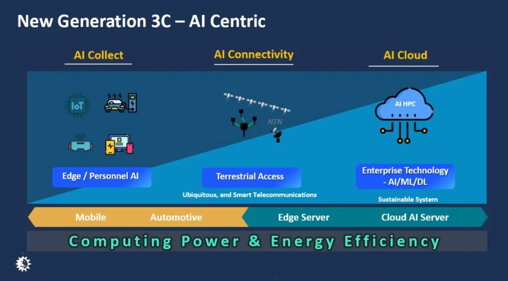
As AI applications become increasingly complex, existing hardware architecture often struggle to achieve higher computing performance while enhancing energy efficiency of data connection across chips and I/Os.
Advanced Packaging for AI Chiplets Integration
The first evolution in AI hardware focuses on using advanced HI packaging to integrate chiplets from diverse wafer nodes, particularly for integrating logic and memory. ASE offers high-density packaging solutions tailored to meet the increasing demand for higher bandwidth and faster data transfer rates in AI and HPC applications. Our offerings include 2.5D&3D IC, Fan Out Chip-on-Substrate (FOCoS) and FOCoS-Bridge.
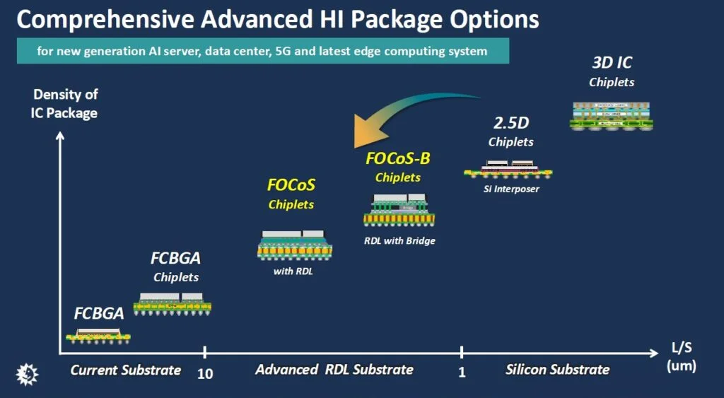
2.5D packaging technology uses a redistribution layer (RDL) on Si Interposer to connect chiplets, achieving a remarkable line width/line spacing (L/S) down to 0.5μm/0.5μm, making it ideal for high-performance applications. FOCoS utilizes fan-out RDL to seamlessly integrate various chiplets, providing a cost-effective solution with an L/S ranging from 2μm/2μm to 10μm/10μm. Lastly, FOCoS-Bridge employs silicon bridges to facilitate high-density routing for connecting different chips, such as logic and memory chips, in areas requiring high-speed transmission, while also utilizing fan-out RDL in other regions. This approach offers flexibility in L/S design, providing both 0.5μm/0.5μm and 2μm/2μm options, while significantly enhancing packaging density and bandwidth.
Advancing AI with Photonic System Integration
Our high-density packaging solutions can achieve a higher I/O density and significantly reduce the interconnection distance between AI chiplets, typically involving around 10 chips. This allows for a more compact design, potentially reducing system size by up to 70%, while also improving overall computing performance by up to 10 times. In the long run, we believe the ideal packaging solution will involve utilizing a full-scale wafer as a single packaged device.
To achieve ExaFLOPS computing power, it requires at least 1,000 AI chiplets interconnected by advanced high-density RDL technology. In the future, there will be AI clusters containing millions of chiplets for complex AI training models, which will require a more efficient method for establishing connections at the system level.
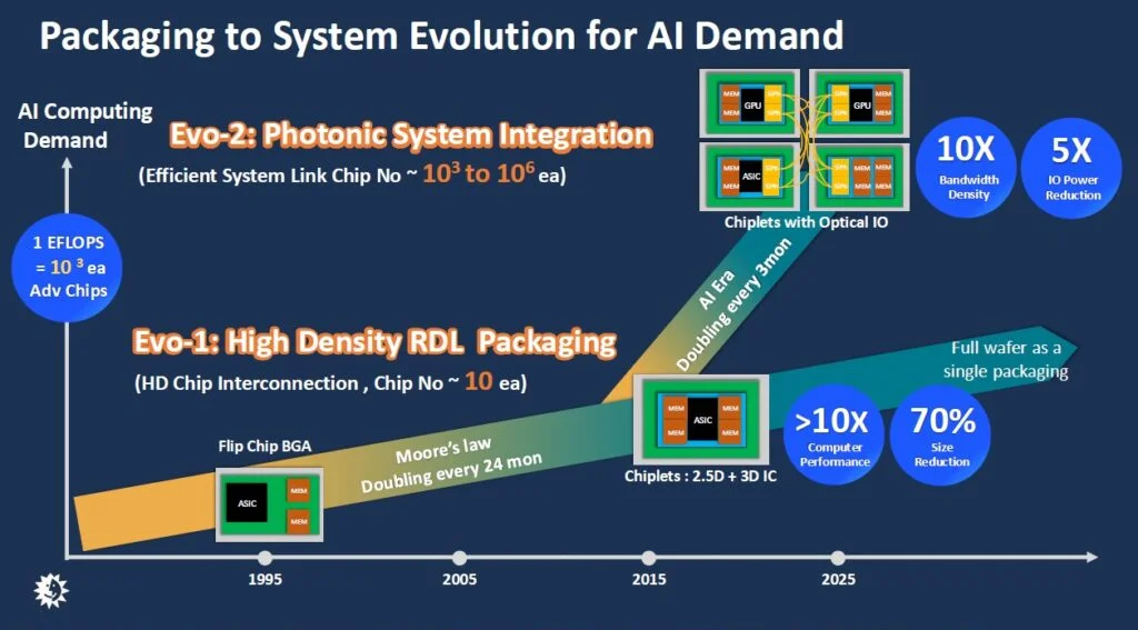
Optical interconnection offers significantly lower transmission losses compared to electrical interconnection, positioning photonic integration as a promising solution for future AI system developments. The industry is witnessing various international programs, such as photonixFAB in Europe, DARPA initiatives in the U.S. and IOWN global forum in Japan, aimed at scaling I/O capabilities while enhancing bandwidth and reducing power consumption. They all focus on a similar approach known as Co-Packaged Optics (CPO).
Complex Assembly Process of Co-Packaged Optics (CPO)
CPO is becoming an enabling technology in the future of AI hardware, primarily serving to interconnect servers in AI Cluster. In a typical CPO configuration for networking, the switch ASIC is centrally positioned, surrounded by multiple photonic engines (also known as optical engines or OEs).
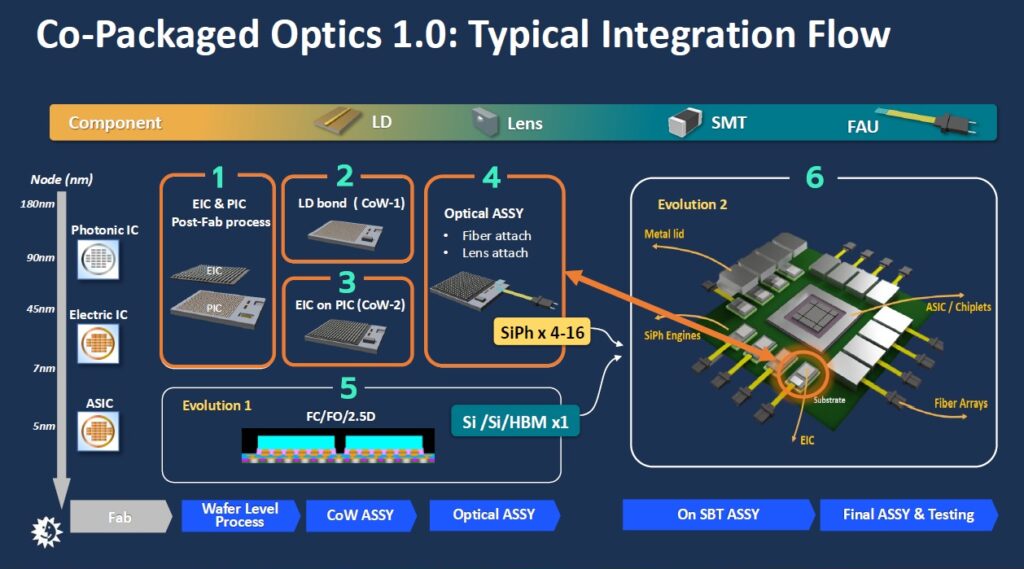
The CPO assembly involves various elements, including lasers, optics, fiber array units (FAUs), and silicon integrated circuits (ICs) with different wafer nodes: photonic integrated circuits (PICs), electronic integrated circuits (EICs), and memory ICs. Some customers require specialized post-CMOS wafer processes, such as deep reactive ion etching (DRIE) cavity formation, AuSn bonding, KOH V-grooves, or fan-out RDL processes.
Ultimately, all the aforementioned elements are integrated on a single packaging substrate, followed by final testing. This results in a highly complex assembly flow, as illustrated in the figure below. The key processes—EIC/PIC 3D integration and fiber assembly—will be discussed in detail later.
Advanced Packaging for EIC/PIC Integration in CPO
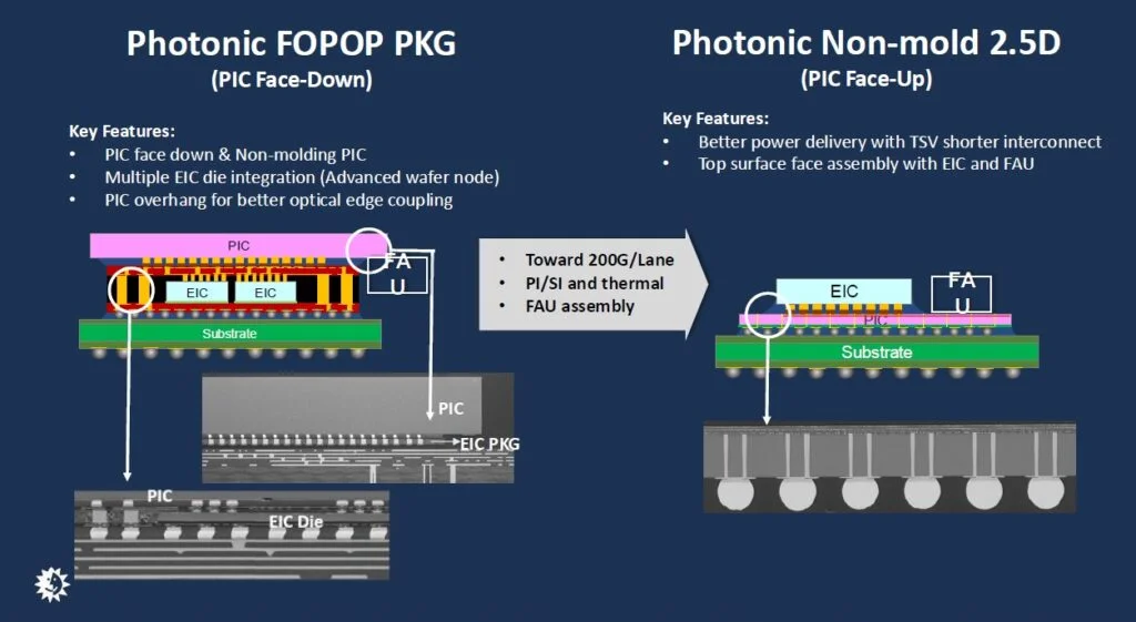
For the integration of EIC and PIC, chip-on-wafer 3D stacking is an effective method to minimize the interconnection distance between the two. This method offers the benefits of a smaller form factor while significantly improving bandwidth density and energy efficiency. Two primary approaches facilitate vertical interconnections: through silicon vias (TSVs) and tall copper pillars in a fan-out package on package (FOPOP) configuration.
Option 1: PIC on Top of EIC
In this configuration, the PIC is placed on top of the EIC. However, creating TSVs in the EIC can be challenging because it usually requires manufacturing at an advanced wafer node. To overcome this, we employ a wafer-level fan-out process that forms tall copper pillars to implement vertical interconnections with the top PIC. The resulting Photonic FOPOP excels in optical coupling, as the overhanging portion of the PIC allows for optical edge coupling.
Option 2: PIC on the Bottom
Alternatively, the PIC can be positioned at the bottom, using TSVs formed therein for vertical interconnections with the top EIC. FAU assembly solution as well as PIC warpage control are crucial for this Photonic Non-mold 2.5D structure. This design offers better thermal dissipation and can achieve higher transmission data rate, for example over 200G per lane, due to better power integrity and signal integrity.
Ultimately, the Photonic Non-mold 2.5D structure offers a superior solution, making PIC with TSV indispensable for silicon photonics.
Fiber to PIC Assembly Solutions
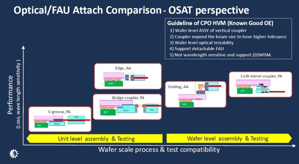
For fiber to PIC integration, there are several key considerations: active alignment, passive alignment, edge coupling, and grating coupling.
To achieve better optical performance — minimizing optical loss and wavelength sensitivity — we believe that edge coupling with active alignment using lenses is the superior choice. However, considering the need for wafer-scale optical testability, a wafer-level solution, such as a chip-on-wafer mirror coupler using passive alignment, may be more suitable for high-volume production.
Therefore, the industry is shifting towards wafer-scale assembly utilizing vertical couplers for optical and FAU assembly in high-volume CPO manufacturing. These couplers can expand the laser beam size, providing greater coupling tolerance. This method allows for wafer-scale testing, supports detachable FAUs, and is less sensitive to wavelength variations, ultimately supporting Dense Wavelength Division Multiplexing (DWDM) systems.
Building a Synergistic Ecosystem
As we navigate this intricate landscape of AI hardware development, it is crucial to establish a synergistic ecosystem among system integrators, design houses, foundries, and OSAT (Outsourced Semiconductor Assembly and Test) providers. The key to success lies in defining specifications clearly and developing known-good optical engines (OE) solutions that can streamline the entire supply chain. The future of AI hardware is filled with promise, with exciting advancements on the horizon. By prioritizing performance, energy efficiency, and innovative packaging solutions, we can unlock the full potential of AI technology and pave the way for a smarter, more efficient world.
Popular Blog Posts

Accelerating the AI Economy through Heterogeneous Integration
2024 / 11 / 21
Advanced Packaging Design for Heterogeneous Integration
2024 / 01 / 26
Welcome to VIPack™
2022 / 06 / 01
Butt-Coupling Optical Probe Card for Wafer-Scale Photonic-Integrated-Circuits Test with Polarization Control
2023 / 09 / 04