post
A Precision Enhancement Deep Learning Framework for Package Substrate Defect Detection
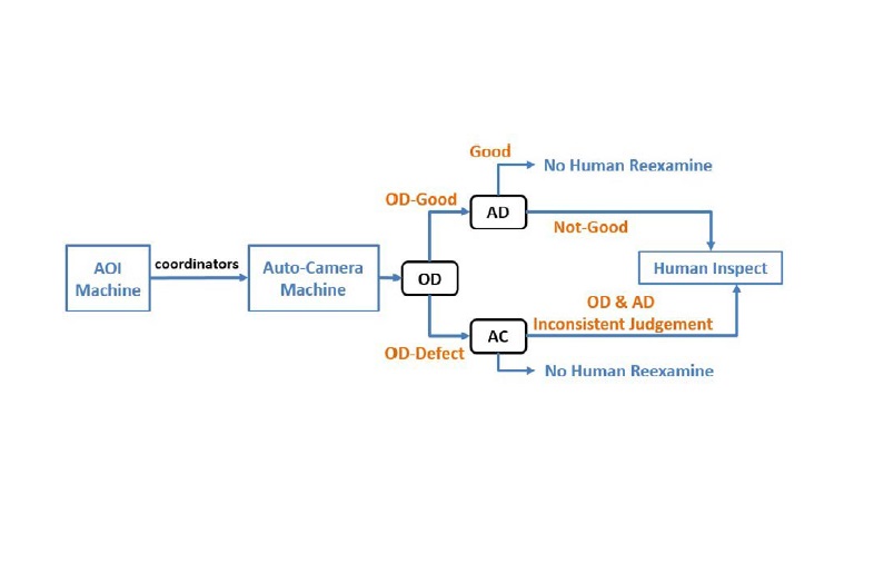
In the manufacturing industry, producing a large quantity of highquality products every day is the top priority. Recently, the integration of Automated Optical Inspection (AOI) equipment and Deep Neural Network (DNN) defect image predictions has demonstrated a significant reduction in manual effort required for defect inspection in manufacturing industrial applications. Read More