Blog
Trends and Development in Heterogeneous Integration: Advancing the Smart Digital Age with System-in-Package and Chiplet Technologies
Evelyn Lu

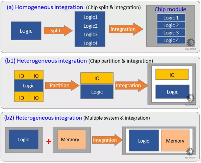
Heterogeneous integration (HI) is fast becoming a key driver of semiconductor development due to its ability to scale the number of individual chips onto a miniaturized system-in-package that enhances functionality, achieves higher efficiency, and even reduces power consumption.
At present, HI technologies are enabled by: system-in-package (SiP) packaging that allows miniaturization and a higher level of integration; 2D/3D IC packaging that delivers higher bandwidth and lower latency; and Fan In/Fan Out Wafer Level Packaging (WLP) that achieves higher performance and higher density. To provide IC designers a robust automated design solution that addresses heterogeneous integration parameters, ASE collaborated with Deca Technologies and Siemens Digital Industries Software to launch the APDK™ (Adaptive Patterning® Design Kit). The APDK methodology provides IC designers a library of templates, extensive automation that guides the designer from initial layout to Adaptive Patterning simulation, to final design sign-off using Siemens’ Calibre software. ASE’s experience in volume production of highly integrated SiP including its M-series Fan-out WLP technology, demonstrates the company’s leadership in advancing device and system performance.
Another trend in HI is the development of chiplets, a relatively inexpensive method that can quickly assemble independent IC chiplets (smaller and usually less expensive chips) through die-to-die interconnect, that when combined, accelerates the performance and power efficiency of the integrated package. An example of a chiplet architecture is the integration of CPU cores, memory ICs and 3D stacking technology to vastly improve bandwidth and interconnect quality. Chiplet designs are gaining popularity as the approach shortens the design leadtime and lowers the cost threshold – IC designers do not need to fabricate new chips using expensive nodes and fab processes. This methodology is now widely applied in designing high-end processors, FPGA and networking ICs.
SPIL (a member of the ASE Technology Holding Co), has developed several fan-out packaging technologies to support chiplets including; Flip Chip Multi-Chip Module (FCMCM), 2.1D/2.5D/3D, Fan Out Multi-Chip Module (FOMCM), Fan-Out Embedded Bridge (FOEB) and Embedded Multi-die Interconnect Bridge (EMIB). The high acceptance rate of these process technologies are contributing to lower manufacturing costs and improving speed to market.
Innovation in the packaging world is game changing, and the combined synergy from ASE, SPIL and USI is raising the company’s competitive edge and industry R&D standards. ASE is also building strong supply partnerships and expanding market opportunities to provide solutions that deliver high performance, speed and efficiency. We sincerely believe that our Heterogeneous Integration journey will contribute immensely to the next generation of smart digital applications.