Press Room
ASE VIPack™ FOCoS-Bridge integrates multiple ASICs and silicon bridges to accelerate AI innovation
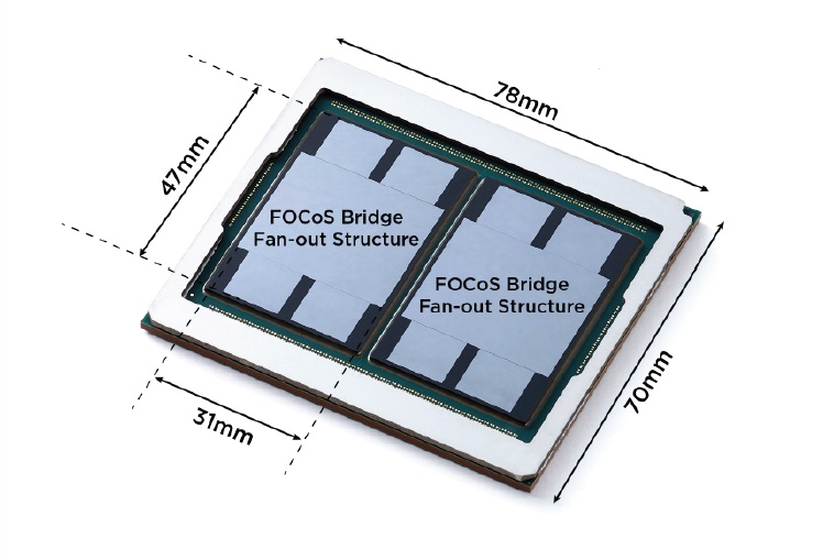
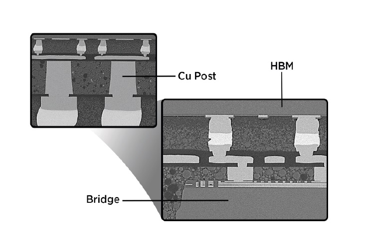
SUNNYVALE, Calif., May 31, 2023 – Advanced Semiconductor Engineering, Inc. (ASE), a member of ASE Technology Holding Co., Ltd. (NYSE: ASX, TAIEX: 3711), today announced its latest Fan-Out-Chip-on-Substrate-Bridge (FOCoS-Bridge) technology breakthrough, achieved through qualifying a large 70mm x 78mm package that incorporates two ASICs and eight High Bandwidth Memory (HBM) devices connected through eight silicon bridges. This large package features two identical 47mm x 31mm FOCoS-Bridge fan-out structures integrated side-by-side, with each comprising an ASIC with four HBMs and four silicon bridges, effectively integrating nine components in each 47mm x 31mm fan-out package, which is almost 2X the silicon reticle size. Positioned under the ASE VIPack™ platform, this FOCoS-Bridge technology is designed to be highly scalable, enabling seamless integration into complex chip architectures while delivering high density die-to-die (D2D) connections, high input/output (I/O) counts, and high-speed signal transmission for evolving Artificial Intelligence (AI) and High-Performance Compute (HPC) requirements.


FOCoS-Bridge technology addresses the increasing demand for higher bandwidth and faster data transfer rates in AI and HPC applications. It leverages the advantages of highly integrated fan-out structures to overcome the limitations of traditional electrical interconnects, and enables high-speed, low-latency, and energy-efficient data communication between processors, accelerators, and memory modules. FOCoS-Bridge establishes the foundation for embedding passives and active chips in the fan-out package and provides options of decoupling capacitor integration for power delivery optimization and active dies for interconnection between to certain functions, such as memory, I/O, and more.
ASE’s FOCoS-Bridge features ultra-high density D2D interconnection with submicron L/S, enabling high bandwidth at low latency for chiplet integration. The use of a silicon bridge die enables a die edge linear density (wire/mm/layer) that is nearly 200x higher than the traditional organic flip chip package. In addition, FOCoS-Bridge enables broad D2D interconnects for both serial and parallel interfaces and associated standards such as XSR, BOW, OpenHBI, AIB, and UCIe.
AI has penetrated nearly all industries and scientific disciplines, from autonomous vehicles to medical diagnostics. The convergence of AI and HPC is having a strong impact on the semiconductor industry, fueling demand for innovative packaging solutions. HPC and server SoCs are approaching maximum reticle sizes and in some cases also require high bandwidth memory integration, which can be enabled by FOCOS-Bridge technology. Furthermore, FOCoS-Bridge technology helps enable more efficient utilization of computing resources, accelerates data-intensive workloads, and contributes to the advancement of AI algorithms, deep learning, scientific simulations, and other computationally demanding tasks.
“FOCoS-Bridge technology is vital for the chiplets era, at a time when industry roadmaps seek novel integration techniques that provide similar electrical signal, and power integrity performance to silicon interposer solutions, but at a lower cost and without reticle size constraints,” said Vikas Gupta, Director of Engineering & Technical Marketing, ASE.
“The breakthrough in FOCoS-Bridge technology pushes the boundaries of AI and HPC by addressing critical challenges related to data communication, performance, and power consumption,” added Dr. C.P. Hung, Vice President of R&D, ASE. “With AI and HPC poised to improve the way we live, work, play, and communicate, we are excited that FOCoS-Bridge and our advanced packaging innovation is playing a key enabling role.”
“ASE is passionate about creating integration technologies that enable our customers to achieve the HBM and high density chiplet integration required to bring their bleeding-edge applications to market,” commented Yin Chang, ASE’s Senior Vice President of Sales & Marketing. “Our creativity continues to deliver transformative solutions such as FOCoS-Bridge, which not only strengthens our VIPack portfolio but also opens up new possibilities for innovation and development in AI, empowering our customers to overcome tough technical challenges and achieve new levels of performance, scalability, and energy efficiency.”
ASE’s FOCoS-Bridge technologies feature within VIPack™, a scalable platform that is expanding in alignment with industry roadmaps.
Supporting resources
- For more about FOCoS-Bridge, please visit: ase.aseglobal.com/focos-bridge/
- For more about VIPack™, please visit: ase.aseglobal.com/vipack/
- Follow us on our LinkedIn page for targeted updates and announcements @aseglobal
- Follow us on Twitter @aseglobal
About ASE, Inc.
Advanced Semiconductor Engineering, Inc. (ASE), a member of ASE Technology Holding Co., Ltd. (NYSE: ASX, TAIEX: 3711) is the leading global provider of semiconductor manufacturing services in assembly and test. Alongside a broad portfolio of established assembly and test technologies, ASE is also delivering innovative VIPack™, advanced packaging, and system-in-package solutions to meet growth momentum across a broad range of end markets, including AI, automotive, 5G, high-performance computing, and more. To learn about our advances in SiP, fanout, MEMS and sensor, flip chip, and 2.5D, 3D and TSV technologies, all ultimately geared towards applications to improve lifestyle and efficiency, please visit: ASE Website , or follow us on LinkedIn & X: @aseglobal.