Blog
Reliability Prediction and Improvement of Board-Level Thermal Cycling Test for Molded Flip-Chip Ball-Grid-Array Package
Dao-Long Chen; Tang-Yuan Chen; Wei-Hong Lai; Wei-Jie Yin; Chun-Liang Kuo; Chun-Yu Ko; Chi-Min Cheng
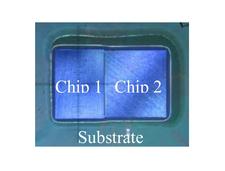
Borrowing the digital twin spirit, the virtual model (CAE simulated) and the physical model (real tests) were used to construct the lifecycle prediction curve for Molded Flip-Chip Ball-Grid-Array Package (MFCBGA) with SAC305 solder ball. The energy based Morrow’s model was used to fit the data points from both virtual and physical models, and the viscoplastic Anand model for the solder material was used to describe the plastic and creep effects. The accuracy is within ±15% with focusing on the one package type, the one temperature condition, and the one solder type.
The lifecycle curve can be used to predict the new devices reliability ahead of the real tests. If the reliability is good, then the real tests can be saved or reduced, and the cost and schedule can thus be saved. If the reliability that predicted is not good, the CAE simulation can be used to improve the reliability.
In this study, the material and structural effects were investigated, and the improvement can be up to 33% for the Board-Level Thermal Cycling Test (BL-TCT).
Published in: 2023 IEEE 25th Electronics Packaging Technology Conference (EPTC)