Blog
Accelerating the AI Economy through Heterogeneous Integration
Yin Chang - Senior Vice President of Sales & Marketing
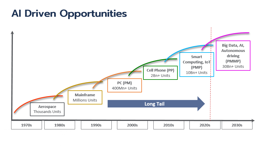
The world is rapidly transitioning from an internet economy to an AI economy. In the internet economy, we stayed constantly connected to the internet 24/7 through our smartphones, PCs, and IoT devices. However, in the AI economy, every aspect of our lives are interwoven with artificial intelligence. You may already be familiar with AI tools such as ChatGPT or Google Gemini, which answer questions and generate human-like text, images and even videos. In the future, multimodal AI can simulate human bio-senses, enabling it to see, hear, and even smell on our behalf. Beyond this, agentic AI will understand its environment, set goals, and take actions with minimal direct human intervention. These are just a few examples of AI’s transformative potential. And as we continue on this journey, we will need greater innovation in semiconductor technology and advanced packaging solutions in order to fully realize the true power of AI.
What will AI bring?
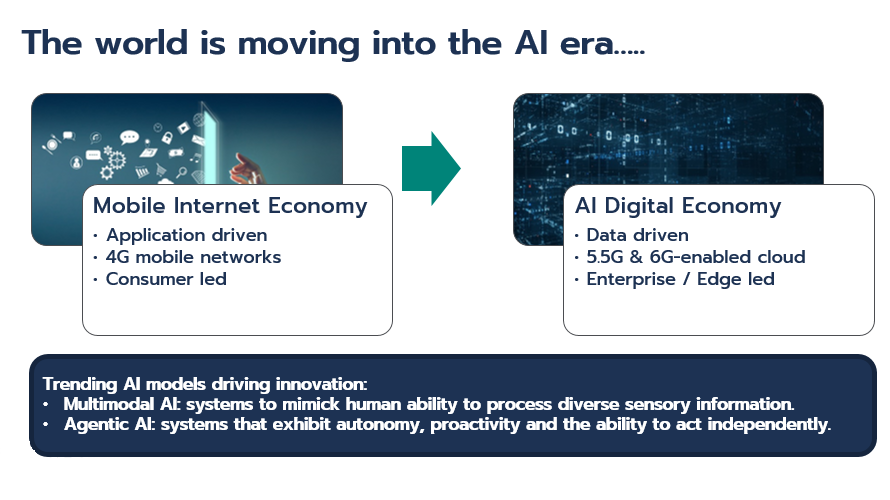
Looking back at the history of technology-driven opportunities, we understand that every technology inflection point has led to a significant increase in the demand for units. Fifty years ago, the aerospace industry required only thousands of units, but with the rise of mobile phones, demand surged to 2 billion units, then smart IoT devices further expanded this to 10 billion units.
We believe AI will drive even greater demand – tripling it to 30 billion units within a relatively short period of time. This growth is being fueled by the emerging people-machine-machine-people (PMMP) communication model where our mobile phone runs various AI applications by interacting with multiple servers and clouds to deliver real-time information and services. These continuous machine-to-machine connections are propelling the semiconductor industry toward a $1 trillion dollar market.
Scaling for the AI Era: Overcoming Challenges with Heterogeneous Integration
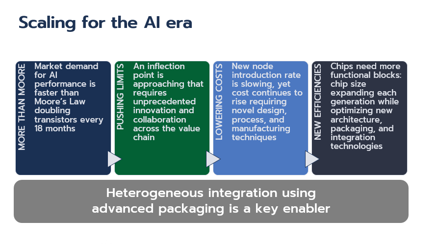
As we enter the AI era, scaling presents significant challenges. The demand for AI and machine learning (ML) performance surged by nearly 6.8x to 11x over a two year period (2021-2022), rapidly outpacing Moore’s Law, which traditionally doubles transistor counts roughly every 18 months.
Power is another critical challenge. Within the next decade, data centers may reach zettabyte scale, consuming up to 500 MW of power to operate, equivalent to half the output of a nuclear power plant. Such high energy consumption is unsustainable, making energy efficiency a priority to support the computational demands of the AI economy.
Cost is also a key concern. Even as the pace of new node introduction slows, production costs continue to rise. The development of a 5nm advanced IC design can now cost nearly half a billion dollars, putting it beyond the reach of many companies.
To achieve the necessary efficiencies, we believe heterogeneous integration is essential. This approach provides a way to reduce power consumption, go beyond More-than-Moore, and lower overall development costs, paving the way for sustainable scaling in the AI era.
Heterogeneous Integration through Advanced Packaging for AI and HPC
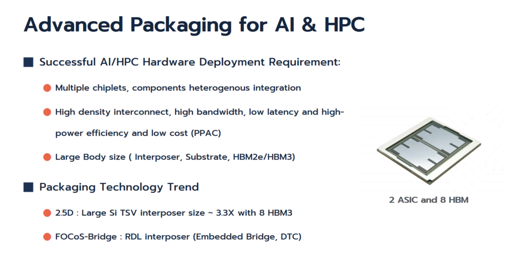
Our advanced packaging technology enables the integration of components made from different materials, process nodes, and technologies into higher-level assemblies like Chiplets, SiPs, and Modules. This approach not only boosts functional density and reduces cost per function but also offers flexibility for system architects to create innovative solutions that enhance Si system performance and efficiency to meet the evolving demands of AI and HPC.
Our next-generation 3D heterogeneous integration architecture, VIPack™, is designed to extend design rules and achieve:
- Maximized clock speed and performance by leveraging best-in-class silicon providers
- Optimized co-design time, development and product time to market
- Open silicon ecosystem in partnership with our foundries/supply chain
VIPack™ comprises six core packaging technology pillars, including high density RDL based FOPoP, FOCoS, FOCoS-Bridge, and FOSiP as well as TSV based 2.5D/3D IC and Integrated Optics processing capabilities. By leveraging our extensive database and our partnerships with EDA vendors (such as Cadence, Synopsys, Xilinx etc.), we have introduced the Integrated Design Ecosystem™ (IDE) enabling our customers to design their packaging solutions faster and more efficiently.
Explore the drawing below for examples of the advanced packaging solutions we have developed for the training GPUs and training AI accelerators.
Conclusion
AI and data continue to fuel semiconductor innovation, with exponential growth through 2030 and beyond, reshaping global life and lifestyle in unimaginable ways. Heterogeneous Integration through advanced packaging has played a pivotal role in enabling the AI economy to transform our world, providing AI chip architects with innovative solutions to optimize chip layout for performance and energy efficiency.
We believe the potential for growth in the AI economy is limitless, and the anticipated $1 trillion dollar semiconductor market is just the beginning. With advanced packaging solutions and continued innovation, we are excited to collaborate with our customers to push the boundaries of possibilities and lead the way in shaping the future of the AI economy.

