Blog
AI and Semiconductor in Reciprocity
Dr. Mike Hung - Senior Vice President, ASE Inc.
In today’s rapidly advancing technological era, AI has become a powerful catalyst for innovation and progress. Advanced semiconductor packaging plays a crucial role in supporting AI development, while AI applications create new semiconductor demands and drives the development of semiconductor technologies, with both complementing each other.
Semiconductor Packaging: The Bridge between Chip and System
The semiconductor market is projected to reach a trillion-dollar by 2030. As wafer technology advances, the L/S (line width/line space) gap between IC and system boards has widened to a phenomenal 2700x compared with an initial 50x. Advanced packaging technology has become essential in bridging this gap. Semiconductor packaging not only provides improvements to system performance but is also a critical foundation for the development of AI. By 2030, the market value of semiconductor packaging alone is expected to reach $150 billion.
Semiconductor Development Trends
The future advancements in semiconductors are primarily centered around three key trends: More Moore, More than Moore, and heterogeneous integration. More Moore is the continuation of Moore’s Law, which aims to scale down transistor size as well as increases transistor density within an integrated circuit while maintaining or enhancing performance. This approach is crucial for the development of GPUs, CPUs, application processors (AP), memory, and logic ICs. More than Moore focuses on the functional diversification of integrated circuits. It emphasizes the development of new materials and functionalities on the chip, playing a vital role in the development of analog, RF, power, passive components, sensors, and even biochips. Heterogeneous integration involves combining various components—such as logic chips, sensors, and memory—to improve system functionality and performance, primarily through two major platforms: advanced packaging and system-in-package (SiP).

Trends in Advanced Packaging for AI
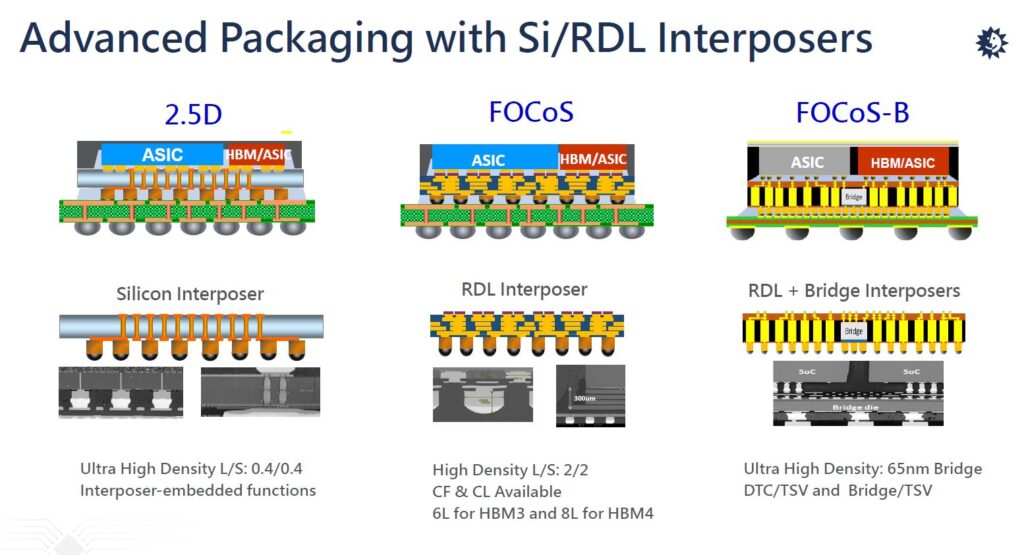
Currently, advanced packaging technologies for integrating AI chiplets, such as GPUs and memory, primarily consist of two platforms: Si Interposer and RDL Interposer. The method of placing chips on a Si Interposer for functional integration is known as 2.5D packaging. In contrast, the RDL Interposer utilizes a redistribution layer (RDL) for functional integration, referred to as FOCoS (Fan Out Chip-on-Substrate) or FO-RDL packaging. If a bridging structure is incorporated within the RDL Interposer, it is termed FOCoS-Bridge or FO-Bridge packaging. For instance, AMD’s MI250 integrates the GPU and HBM on an RDL Interposer, employing the embedded silicon bridge to create fine-line connections between the GPU and HBM.
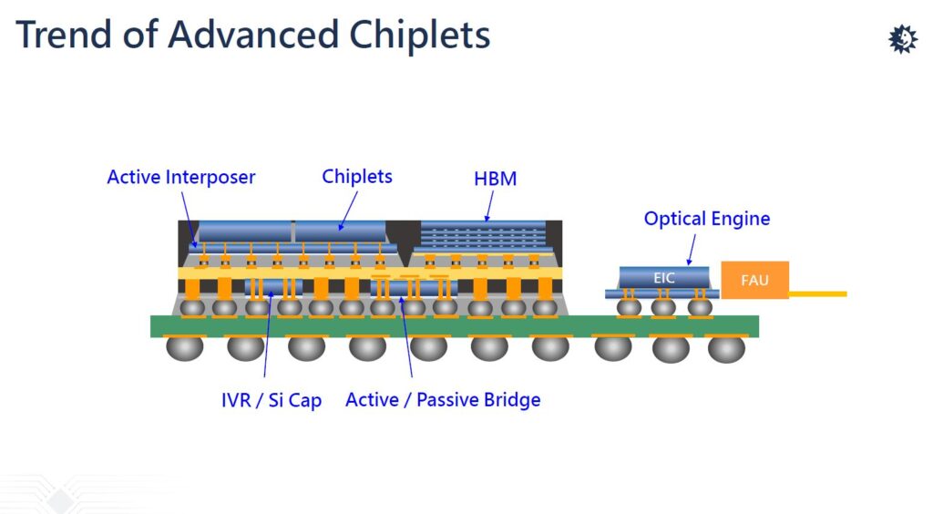
Looking ahead at future trends in advanced packaging, active interposers with transistors will gradually take the place of passive interposers, and FO-Bridge technology will become widely adopted. For example, the packaging design for memory stacked on ASICs, ASICs stacked on memory, or EICs stacked on Photonics ICs (PICs) features chiplet integration on active silicon interposers. This shift from passive to active interposers drives the transition from horizontal arrangements to vertical stacking. Moreover, signal transmission will gradually shift from copper wire connections to optical connections that provide nearly unlimited bandwidth.
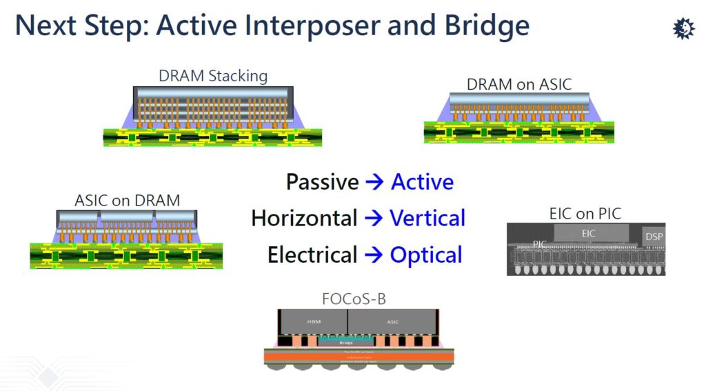
With the rise of chiplet integration, the advanced packaging for AI will include multiple 3D ICs and other components (such as integrated voltage regulators (IVR) and silicon capacitors (Si-Cap)), and optical engines will be integrated to further enhance system performance.
System-in-Package Integration Trends
In the era of the Internet of Things (IoT), system-in-package (SiP) technology plays a crucial role in driving innovation. In applications like smart homes, wearable devices, industrial automation, and smart cities, it is essential to integrate various functions, including data collection, processing, and communication, at the system level. SiP technology enables the integration of multiple components — such as processors, sensors, wireless transmission modules, and power modules — into a single package, streamlining design and enhancing system efficiency. As the functions of system integration expand, the quantity of components in SiP is rising, with SiPs now commonly integrating 300 to over 500 components.

AI Drives Transformative Demands for Semiconductors
As AI applications become increasingly integrated into daily life, PMMP (People-Machine-Machine-People) is emerging as the primary mode of interaction. Beyond traditional human-machine interactions, AI enables extensive communication and collaboration between machines, significantly boosting semiconductor demand across various sectors, including 5G and smart devices, autonomous driving, high-performance computing in data centers, and edge devices. This trend is continuously fostering innovation and growth across the semiconductor industry.
Conclusion: Collaborating towards a Symbiotic Future
The semiconductor industry, driven by continuous scaling in line with Moore’s Law as well as utilizing advanced packaging technologies, plays a crucial role in providing the computing power required for AI development. Meanwhile, the rise of new AI applications generates substantial new demand for semiconductors. The relationship between AI and semiconductors is symbiotic, complementing each other like fish and water. As demand continues to rise, this positive cycle will propel continuous innovation and advancement in the semiconductor industry. We look forward to embracing a future, full of opportunities together.

