Blog
Integrated Design Ecosystem™ for Chiplets and Heterogeneous Integration in Advanced Packaging Technology
Dr. Lihong Cao, Sr. Director of Technology & Business Development
As the demand for high-performance computing (HPC) continues to grow, chiplets and heterogeneous integration have emerged as key solutions due to their significant advantages in improving yield, reusing IP, enhancing performance, and optimizing costs. The integration of chiplets, particularly for AI applications, necessitates a greater number of connections than traditional monolithic system-on-chip (SoC) designs. These connections must ensure high density, efficient data transfer, and effective power delivery. This has led to an increased demand for advanced packaging that features a higher number of interconnects and larger body sizes. The layout density of these packages can be tens to hundreds of times greater than that of conventional FCBGA packages. The high density and complex connectivity in advanced packaging introduce new challenges for packaging design and assembly manufacturing validation.
To address these challenges, ASE has developed the Integrated Design Ecosystem™ (IDE), a collaborative design toolset optimized to enhance advanced package architecture across its VIPack™ platform. The IDE facilitates a smooth transition from single-die SoCs to multi-die disaggregated IP blocks, including chiplets and memory, using 2.5D or advanced fan-out structures.
Package Design Challenges for Chiplets Integration
Traditionally, IC chip design and package layout design have been planned and executed separately for monolithic SoC with FCBGA package. However, as the transition from single monolithic SoCs to multi-chiplet architectures becomes inevitable, designers face increasing challenges in optimizing the interconnections between chiplets to enhance performance, making the design process significantly more complex. Furthermore, the die-to-die interconnects for chiplets integration are often proprietary links from various customers, which creates further design constraints and hinders the adoption of advanced packaging technologies.
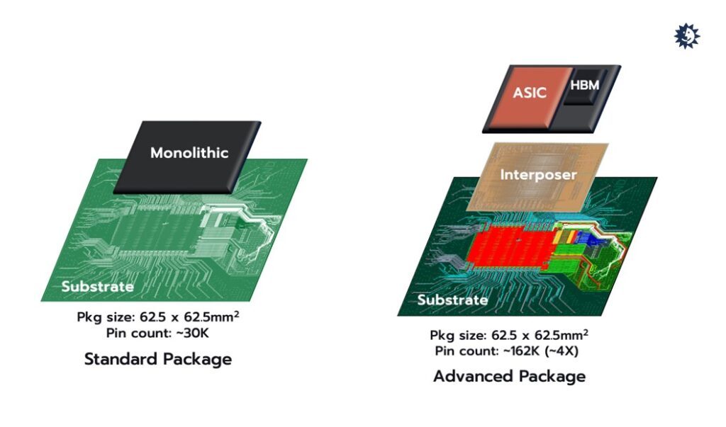
For instance, as illustrated in the picture below, a standard FCBGA package for a monolithic die measures 62.5 x 62.5 mm² and has around 30,000 I/O pins. In contrast, when using chiplets — such as one ASIC die and one high-bandwidth memory (HBM) — a silicon interposer or redistribution layer (RDL) interposer is required to integrate the chiplets. While the size of the advanced package remains the same, the number of pins can increase fourfold to approximately 160,000.

Designing ultra-high I/O density routings for the Si interposer or RDL interposer necessitates layout design rule checks (DRC) and Layout Versus Schematics (LVS) tools, which are often unavailable in traditional package design tools. As a result, the design cycle time can increase by a factor of ten compared to standard packaging design for monolithic die.
For monolithic dies, the focus has typically been on board-level design, including PCB and substrate design, while foundries have concentrated solely on the chip and silicon design. However, for chiplet integration, these aspects cannot be addressed in isolation; they must be considered holistically. Therefore, there is a need to develop a design platform that facilitates system-level optimizations for power, performance, and area (PPA) in chiplet and heterogeneous integration. This platform should be capable of aggregating data from IC designers, package designers, and even board designers.
ASE Integrated Design Ecosystem™
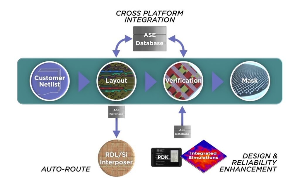
We have introduced the Integrated Design Ecosystem™ (IDE) to address the package design challenges associated with chiplet integration, significantly enhancing both design efficiency and quality while also reducing time-to-market for our customers. Key features of our IDE include cross-platform interaction for layout and verification, advanced automated routing for RDL and silicon interposers with built-in design rule checking (DRC), and the implementation of a Package Design Kit (PDK) within the design workflow.

The IDE supports a range of chiplets interconnection standards, including serial I/O connections like extra short-reach (XSR) and SerDes, as well as parallel I/O connections such as Bunch of Wires (BoW), Open High Bandwidth Interconnect (openHBI), and Universal Chiplet Interconnect Express (UCIe). This will allow different chiplet designers to create discrete chiplets that can interoperate seamlessly. Compared to traditional design platforms, the IDE can improve design efficiency by up to 50% and enhance design accuracy.
Integrating IDE into ASE’s Packaging Design Workflow
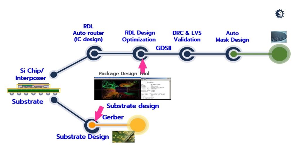
The IDE is ideal for optimizing the design of chiplets integration using our FOCoS RDL interposer or 2.5D Si interposer. As shown in the figure below, the process begins with substrate design, where we utilize a conventional package design tool to create a global file. For the interposer design, we employ an IC design tool for automated routing, and transition back to the package design tool to optimize the RDL design and generate the Graphical Design System (GDS) file for design verification, which includes DRC and LVS validation. Finally, we use an automated mask design process to create the RDL mask for the fan-out wafer or RDL wafer manufacturing.

In the case of FOCoS design, when we receive the netlist or relative coordinates, it usually takes several weeks to complete the RDL routing using traditional package design tools. However, by leveraging the auto router and IC design tool, we can reduce the total interposer layout design cycle time by 50% or more. Additionally, our automated mask generator significantly shortens the design lead time for the RDL mask from three days to less than one hour.
ASE Design Turnkey Solutions for Chiplets and Heterogeneous Integration
In today’s rapidly evolving technological environment, chiplets and heterogeneous integration are improving system performance, extending the scalability of Moore’s law, and enabling AI to play a crucial role in high-performance computing (HPC), AI/ML, cloud computing, automotive technology, and 5G. For chiplets to be widely adopted, interoperability and plug-and-play capabilities are vital. The ASE Integrated Design Ecosystem (IDE) has been developed to provide IC and system designers with a comprehensive turnkey solution that encompasses the entire process — from interposer design and stress simulation to manufacturing feasibility validation — ensuring the successful integration of multiple chiplets into a single package while optimizing system performance.


