Blog
Welcome to VIPack™
Mark Gerber
There are still many unknowns as we continue through challenging global times. However, it is inspiring to see such game-changing innovation within the semiconductor industry, ultimately enabling applications that are literally changing lives, from health to transportation, from robotics to AI, from edge to cloud, from 5G to beyond. Collectively, we are helping to improve lifestyles and efficiencies by creating a smarter and more sustainable world for generations to come.
ASE is blazing new trails in device miniaturization and integration, and ongoing innovation means we are delivering advanced packaging and System-in-Package solutions to meet growth momentum across a broad range of end markets, such as automotive, 5G, AI, IoT, high performance computing, and more.
In recent times, we have presented many solutions for SiP. Today we present ViP, or VIPack™, an advanced packaging platform designed to enable vertically integrated package solutions. VIPack™ represents ASE’s next generation of 3D heterogeneous integration architecture that extends design rules and achieves ultra-high density and performance. The platform leverages advanced redistribution layer (RDL) processes, embedded integration, and 2.5D and 3D technologies to help customers achieve unprecedented innovation when integrating multiple chips within a single package. To summarize, the VIPack™ platform enables heterogeneous integration through multi stack RDL layered package structures.
ASE’s VIPack™ addresses the following device challenges: insertion loss, integration challenges, clock/speed, height, power delivery, and dense IO, all very critical area, and it is specifically geared towards mobile, high-performance computing, networking, and RF.
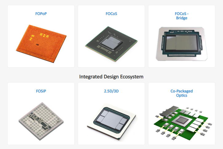
The VIPack™ platform comprises six core packaging technology pillars supported by a comprehensive and integrated design ecosystem. These technology pillars include ASE’s high density RDL based FOPoP, FOCoS, FOCoS-Bridge, and FOSiP as well as TSV based 2.5D/3D IC and Co-Packaged Optics processing capabilities. It provides vast capabilities necessary to enable the next generation highly integrated silicon packaging solutions required to optimize clock speed, bandwidth, power delivery and the ability to optimize co-design time, product development and time to market. Such includes Double Sided RDL/Fan-Out, RDL Integrated Passives, Ultra Dense Routing, Advanced Materials, and DTC Integration.
VIPack™ touches most market segments and has many sub-package platforms where high performance is needed or alternative solutions to ABF/Substrate based routing. It will extend most advanced package technology roadmaps and there are significant cost and performance advantages when considering VIPack™.
Ultimately, today’s advanced silicon nodes are pushing the limits of power delivery where noise and performance are critical while managing overall power. VIPack™ enables a suite of packaging solutions, addressing multiple market segments, that are targeted to provide solutions to these challenges and enable an extension to advanced packaging roadmaps.
We welcome you to discuss VIPack™ with us!
For more about VIPack™, please visit ase.aseglobal.com/vipack